

Vertical-type semiconductor device
a semiconductor device and vertical-type technology, applied in the direction of semiconductor devices, electrical equipment, transistors, etc., can solve the problems of difficult control of mos transistors by gates, leakage current properties and threshold voltages in vertical-type pillar transistors formed in each of the semiconductor patterns, and difficult to ensure electrical properties of vertical-type pillar transistors. , to achieve the effect of high performan
- Summary
- Abstract
- Description
- Claims
- Application Information
AI Technical Summary
Benefits of technology
Problems solved by technology
Method used
Image

Examples
embodiment 1
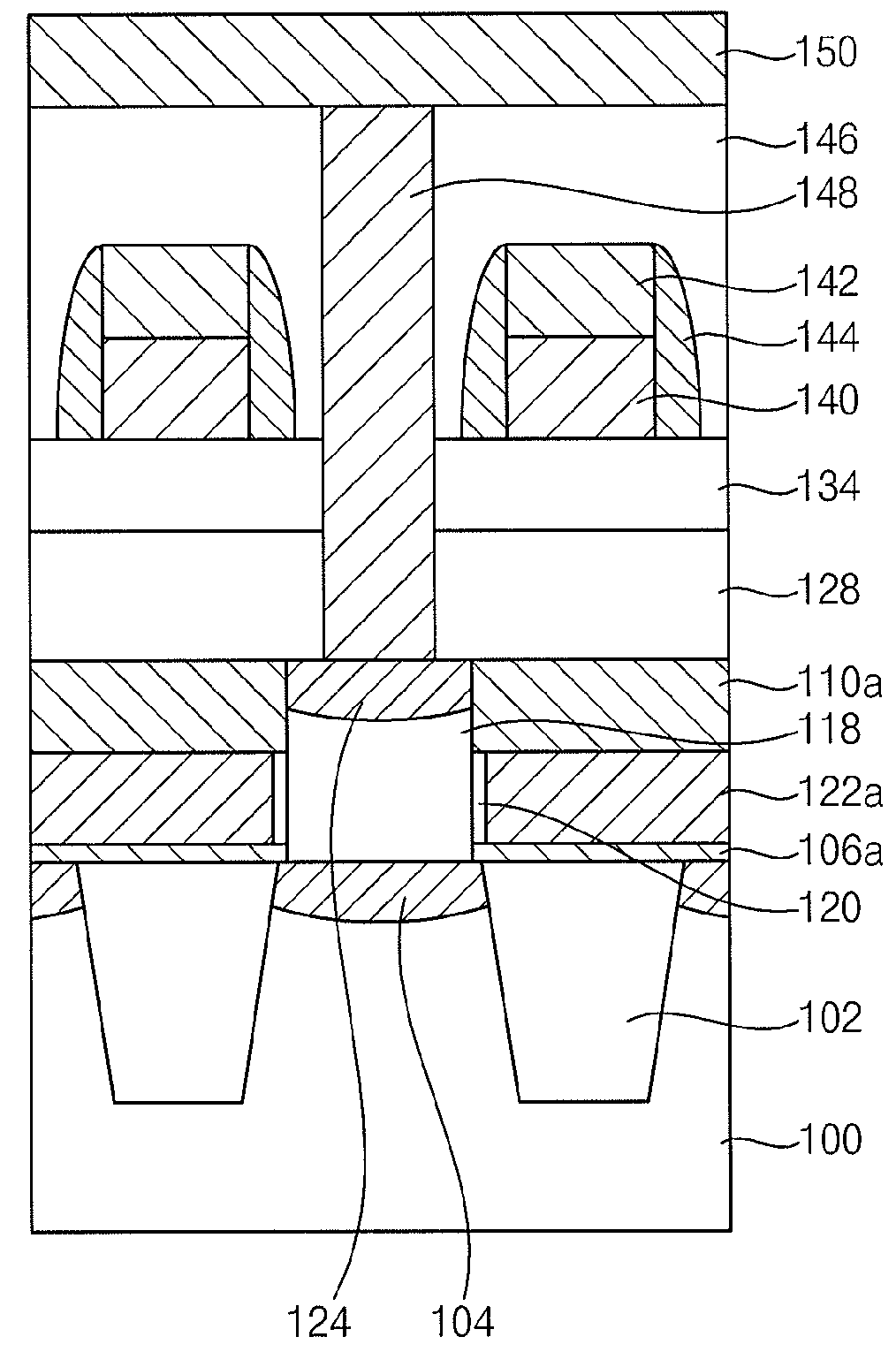
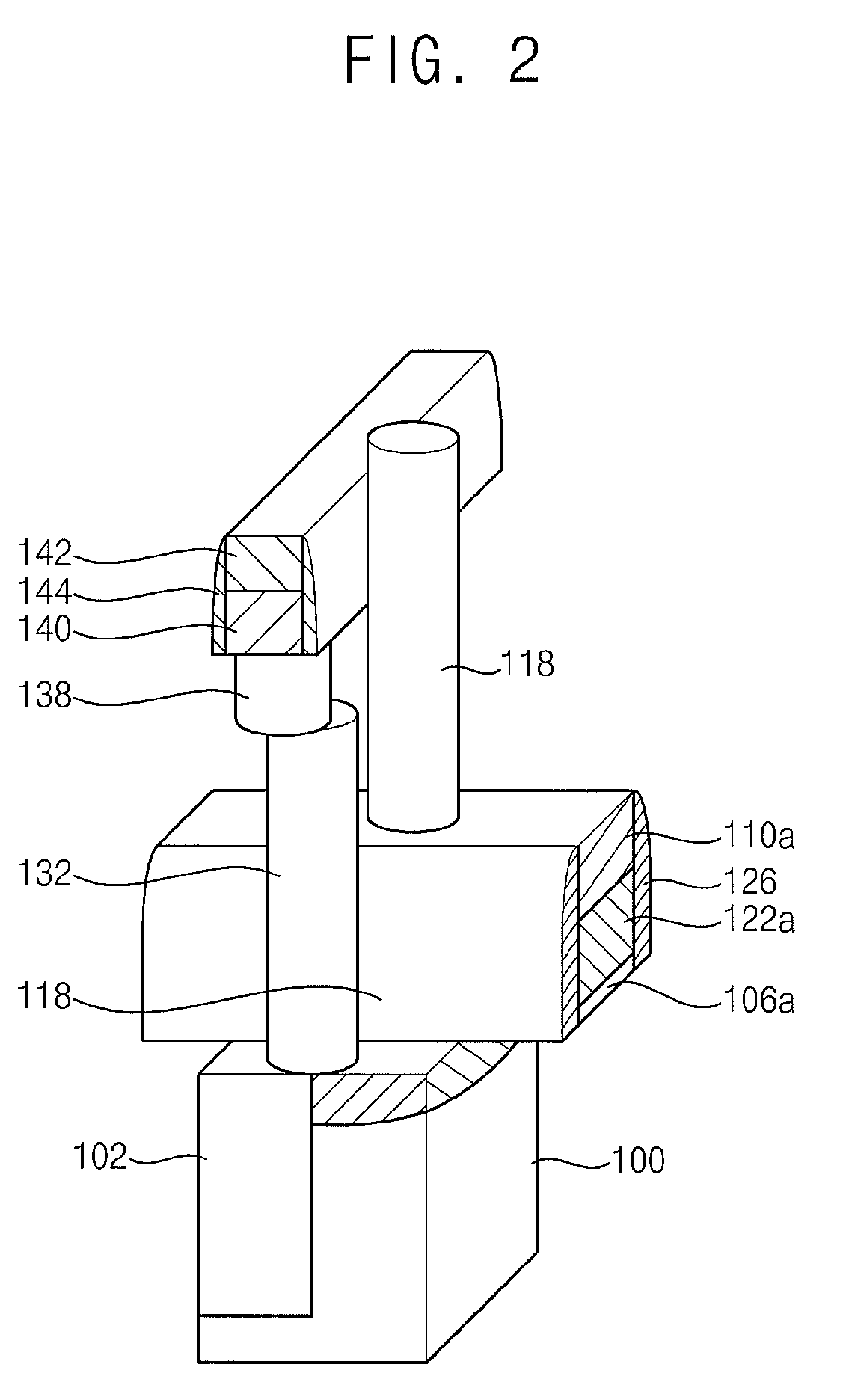
[0062]FIG. 1 is a cross-sectional view illustrating a DRAM device including a vertical-type pillar transistor in accordance with a first example embodiment. FIG. 2 is a perspective view illustrating the DRAM device in FIG. 1.
[0063]Referring to FIG. 1, a substrate 100 having an active region and an isolation region is prepared. The substrate 100 may include single-crystalline semiconductor material. For example, the substrate 100 may include single-crystalline silicon. Trenches are formed in the isolation region of the substrate 100. An isolation layer pattern 102 is formed in the trench.
[0064]The active region and the isolation region extend in a first direction. The active region and the isolation region having linear shapes are arranged alternately with one another.
[0065]A single-crystalline semiconductor pattern 118 having a pillar shape is provided on the active region of the substrate 100. The single-crystalline semiconductor pattern 118 may includes single-crystalline silicon....
embodiment 2
[0159]FIG. 28 is a cross-section view illustrating a DRAM device including a vertical-type pillar transistor in accordance with a second example embodiment.
[0160]A vertical-type pillar transistor, a bit line and a contact plug of a DRAM device according to the present embodiment are substantially the same as in Embodiment 1. However, unlike the DRAM device in Embodiment 1, a capacitor 208 is provided on an upper surface of the contact plug in Embodiment 2.
[0161]The capacitor 208 includes a lower electrode 202, a dielectric layer 204 and an upper electrode 206. The lower electrode 202 and the upper electrode 206 may include metal. Alternatively, the lower electrode 202 and the upper electrode 206 may include polysilicon.
[0162]As illustrated in the figure, the lower electrode 202 may have a cylindrical shape. In this case, a contact area between the dielectric layer 204 and the lower electrode 202 may be increased to provide a higher capacitance.
[0163]Although it is not illustrated in...
embodiment 3
[0176]FIG. 29 is a cross-section view illustrating a memory device including a vertical-type pillar transistor in accordance with a third example embodiment.
[0177]A vertical-type pillar transistor, a bit line and a contact plug of a memory device according to the present embodiment are substantially the same as in Embodiment 1. However, unlike the DRAM device in Embodiment 1, a phase changeable structure 254 is provided on an upper surface of the contact plug.
[0178]The phase changeable structure 254 has a staked structure of a phase changeable layer pattern 250 and an upper electrode 252. For example, the upper electrode 252 may include metal. For example, the upper electrode 252 may include tungsten, titanium, titanium nitride, tantalum, tantalum nitride, molybdenum nitride, niobium nitride, titanium silicon nitride, aluminum, titanium aluminum nitride, titanium boron nitride, zirconium aluminum nitride, molybdenum silicon nitride, tungsten boron nitride, zirconium aluminum nitride...
PUM
 Abstract
Description
Claims
Application Information