Organic solar cells and method of manufacturing the same

a solar cell and organic technology, applied in the field of organic solar cells, can solve the problems of inability to artificially manufacture inability to obtain such an ideal structure, and difficulty in manufacturing an ideal electron donor/acceptor structure, etc., and achieve the effect of increasing electrons

Inactive Publication Date: 2009-12-24
KOREA ADVANCED INST OF SCI & TECH
View PDF12 Cites 40 Cited by
  • Summary
  • Abstract
  • Description
  • Claims
  • Application Information

AI Technical Summary

Benefits of technology

[0016]Leading to the present invention, thorough research carried out by the present inventors aiming to solve the problems encountered in the related art resulted in the finding that, when an organic solar cell is manufactured by forming nano patterns on a photoactive layer using a nanoimprinting process and then applying a cathode electrode material on the photoactive layer having the nano patterns so that a cathode electr

Problems solved by technology

However, the bulk-heterojunction structure is problematic because excitons which are electron-hole pairs formed in the electron donor such as a conductive polymer by solar light have a diffusion distance of only about 10 nm in the polymer, and thus they are recombined and disappear when not reaching the interface between the electron donor and the electron acceptor within the above distance.
Further, such an electron donor/acceptor structure is not externally artificially determined, but is set by the type of solvent, composition of the mixture, spin coating conditions, drying conditions, thermal treatment conditions, and the other post treatment conditions and mainly depends on self-assembling properties of the conductive polymer, thus making it difficult to manufacture an ideal electron donor/acceptor structure.
However, the electron donor/acceptor structure cannot be artificially determined but is dependent on phase separation properties after the mixing of materials, thus making it impossible to obtain such an ideal structure.
Also, in the case where the electron donor and the electron acceptor are mixed in similar amounts, an electron donor-rich region consti

Method used


Image

  • Organic solar cells and method of manufacturing the same
  • Organic solar cells and method of manufacturing the same
  • Organic solar cells and method of manufacturing the same

Examples


example 1

Manufacturing of Organic Solar Cell Using Nanoimprinting After Drying of Photoactive Layer

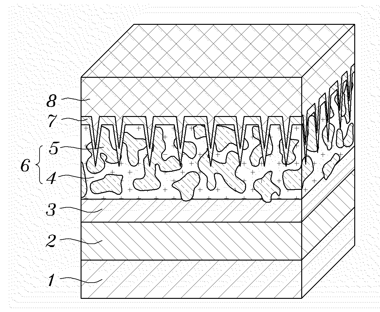
[0053]1-1: Formation of Hole Transfer Layer

[0054]A glass substrate coated with ITO was washed with acetone and alcohol using a sonicator, and then subjected to plasma treatment using an oxygen plasma generator (PDC-32G, available from Harrick Plasma) in an oxygen atmosphere to thus remove organics from the surface thereof. A hydroxyl group was formed on the surface of ITO, so that the ITO surface was made hydrophilic. Subsequently, poly(3,4-ethylenedioxythiophene)-polystyrenesulfonate (available from Bayer) was applied on the hydrophilic surface of ITO through spin coating and then dried at 140° C., thus completely removing the solvent, thereby forming a hole transfer layer on the glass substrate.

[0055]1-2: Formation of Photoactive layer

[0056]30 mg of an electron donor material, for example, poly-3-hexylthiophene (P3HT) and 21 mg of an electron acceptor material, for example, PCBM were dissolve...

example 2

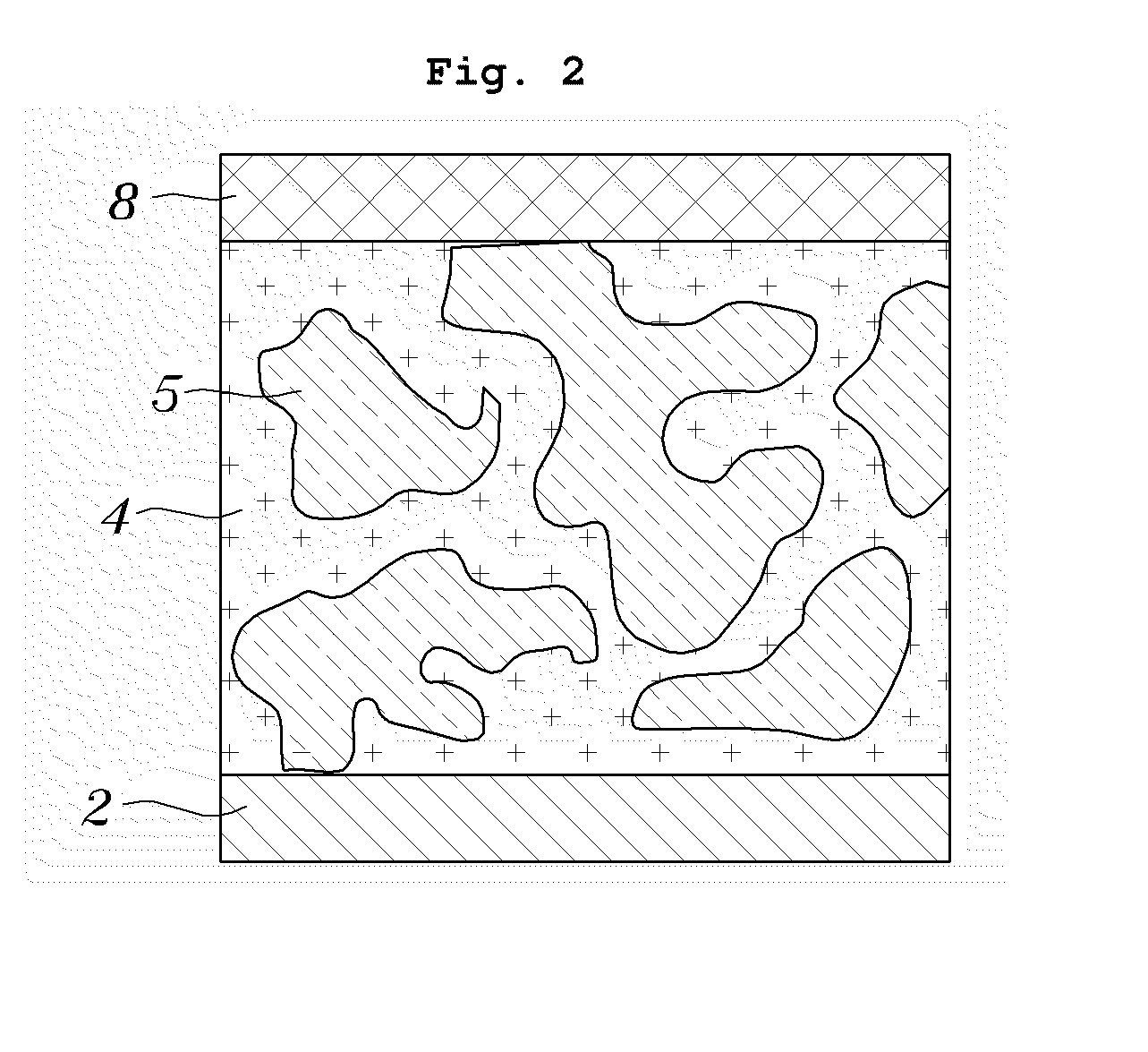
Manufacturing of Organic Solar Cell Using Nanoimprinting before Drying of Photoactive Layer

[0061]An organic solar cell was manufactured in the same manner as in Example 1, with the exception that, in Example 1-2, the mixture of the photoactive layer applied on the hole transfer layer was not dried, and the solvent of the mixture was dried in a state in which the mold was placed on the mixture of the photoactive layer directly after application of the mixture.

experimental example 1

Comparison of Characteristics of Solar Cells

[0064]The current-voltage characteristics of the organic solar cells manufactured in Examples 1 and 2 and Comparative Examples 1 and 2 were compared using a solar simulator (66984 available from Newport). As the solar simulator, a 300 W xenon lamp (6258 available from Newport) and an AM1.5G filter (81088A available from Newport) were used, and the intensity of light was set to 100 mW / cm2.

[0065]As is apparent from the results shown in Table 1 and FIG. 7, the organic solar cells of Examples 1 and 2 had very high short-circuit current compared to the organic solar cells of Comparative Examples 1 and 2. Further, in the evaluation of the effect of the thermal treatment for making the photoactive layer flexible during the nanoimprinting process of Example 1 on improvement of the short-circuit current, because the solar cell of Comparative Example 2 which was thermally treated at 150° C. for 2 min without the use of the mold had no power conversi...


PUM

PropertyMeasurementUnit
Lengthaaaaaaaaaa
Forceaaaaaaaaaa
Electrical conductivityaaaaaaaaaa

Abstract

An organic solar cell and a method of manufacturing the same. This invention relates to a method of manufacturing an organic solar cell including forming nano patterns on a photoactive layer using a nanoimprinting process, and applying a cathode electrode material on the photoactive layer having the nano patterns so that the cathode electrode material infiltrates the nano patterns of the photoactive layer, thus increasing electron conductivity and efficiently forming a pathway for the transfer of electrons, and to an organic solar cell manufactured through the method. This method reduces loss of photocurrent occurring as a result of aggregation of an electron acceptor material and improves molecular orientation of an electron donor in the nanoimprinting process to thus increase cell efficiency. Thereby, the organic solar cell having high efficiency is manufactured at low cost through a simple manufacturing process. The method can be applied to the fabrication of organic solar cells which use an environmentally friendly and recyclable energy source.

Description

CROSS-REFERENCES TO RELATED APPLICATION[0001]This patent application claims the benefit of priority under 35 U.S.C. §119 of Korean Patent Application No. 10-2008-0057357 filed on Jun. 18, 2008, the contents of which are incorporated herein by reference.BACKGROUND OF THE INVENTION[0002]1. Field of the Invention[0003]The present invention relates to an organic solar cell and a method of manufacturing the same. More particularly, the present invention relates to a method of manufacturing an organic solar cell, including forming nano patterns on a photoactive layer of the organic solar cell using a nanoimprinting process, and applying a cathode electrode material on the photoactive layer having the nano patterns so that the cathode electrode material infiltrates the nano patterns of the photoactive layer, thus increasing electron conductivity and efficiently forming a pathway for the transfer of electrons, and to an organic solar cell manufactured through the above method.[0004]2. Descr...

Claims


Application Information

Patent Timeline
IPC IPC(8): H01L51/44H01L51/48H01L51/46
CPCB82Y10/00H01L51/0023H01L51/0036H01L51/0037Y02E10/549H01L51/4253H01L51/442H01L51/447H01L51/0047Y02P70/50H10K71/621H10K85/1135H10K85/215H10K85/113H10K30/87H10K30/82H10K30/30H10K30/00
Inventor JUNG, HEE TAELEE, JAE HYUNKIM, DAE WOOJANG, HONG
Owner KOREA ADVANCED INST OF SCI & TECH
Why Eureka
Try Eureka