Method of cleaning film forming apparatus and film forming apparatus

Inactive Publication Date: 2010-01-21
LAIR LIQUIDE SA POUR LETUDE & LEXPLOITATION DES PROCEDES GEORGES CLAUDE
View PDF13 Cites 113 Cited by
  • Summary
  • Abstract
  • Description
  • Claims
  • Application Information

AI Technical Summary

Benefits of technology

[0017]According to the present invention, the deposit containing tantalum nitride, titanium nitride, tantalum, or titanium adhering to the wall of the processing chamber of the film forming apparatus can be removed uniformly at a high etching rate. When a

Problems solved by technology

The deposited reaction product containing TaN or TiN is peeled from the inner wall or the like of the processing chamber, thereby resulting in generation of particles.
The particles adhere to the semiconductor wafer at the time of next formation of the TaN or TiN film on the semiconductor wafer, thereby deteriorating the quality of the TaN or TiN film.
However, this method needs complicated long cleaning treatment of cleaning the processing chamber with the acid solution, washing with water, and removing water after

Method used


Image

  • Method of cleaning film forming apparatus and film forming apparatus
  • Method of cleaning film forming apparatus and film forming apparatus

Examples


examples 1 to 6

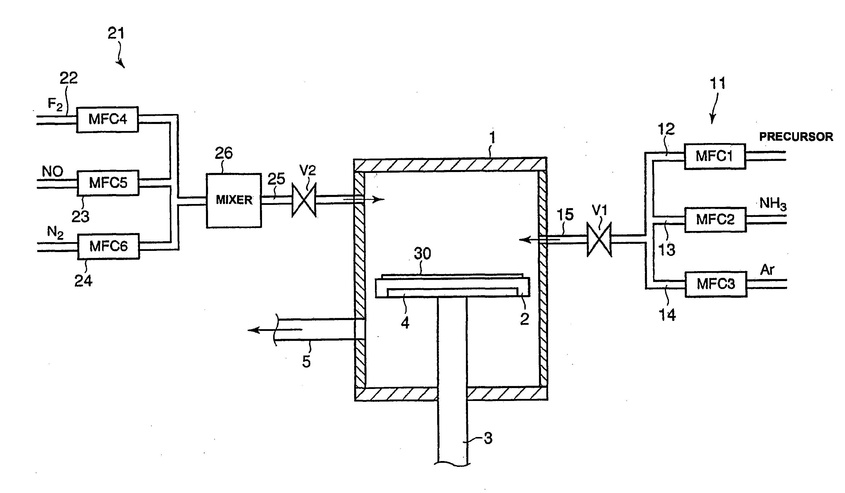
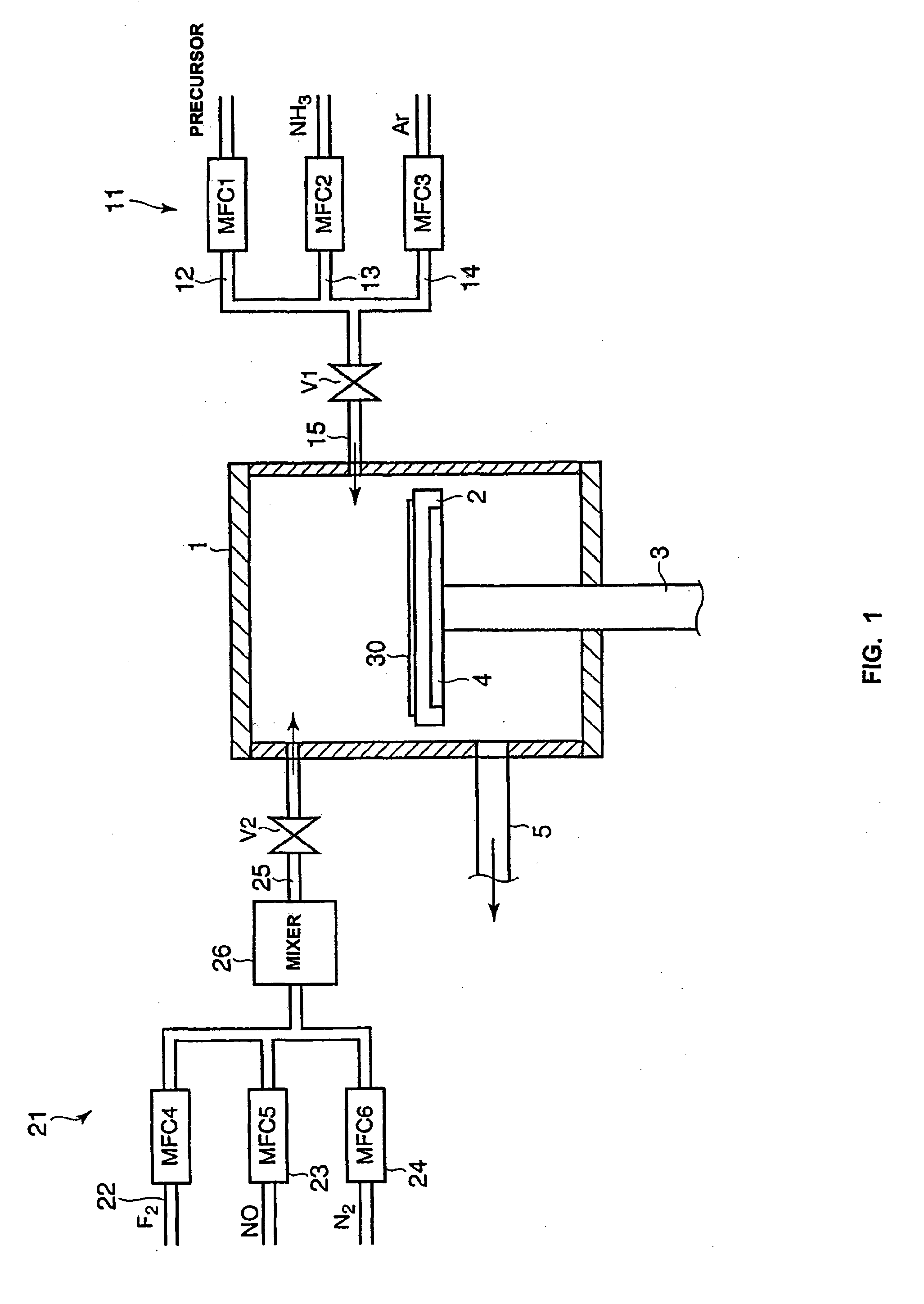
[0043]A tantalum nitride thin film (TaN thin film) of 2000 Å in thickness was formed on an aluminum sheet surface so as to produce a sample. The sample was carried onto the susceptor 2 within the processing chamber 1 of the film forming apparatus shown in FIG. 1. Subsequently, fluorine gas (F2) and nitrogen (N2) gas were supplied into the processing chamber 1 from the process gas supply means 21, and cleaning was carried out under the following conditions.

[0044]Conditions of Examples 1 to 3[0045]Gas mixture: 20% by volume of F2—N2 [0046]Flow rate of mixed gas: 1 slm[0047]Pressure in processing chamber: 5 Torr (Example 1), 10 Torr (Example 2) and 40 Torr (Example 3)[0048]Sample heating temperature: 200° C.

[0049]Conditions of Examples 4 to 6[0050]Gas mixture: 20% by volume of F2—N2 [0051]Flow rate of mixed gas: 1 slm[0052]Pressure in processing chamber: 5 Torr (Example 4), 10 Torr (Example 5) and 40 Torr (Example 6)[0053]Sample heating temperature: 300° C.

[0054]Etching velocity of the...

examples 7 to 10

[0056]The etching velocity of the TaN thin film of the sample was measured according to the same method as Example 2 except that the same sample as Examples 1 to 6 was heated to temperatures of 100° C., 250° C., 350° C., and 500° C. Table 2 shows the result. In the meantime, Table 2 includes Example 2 and Example 5 of the Table 1.

TABLE 2HeatingEtching ratetemperature (° C.)(Å / min)Example 71005Example 220012Example 8250168Example 5300220Example 9350485Example 105001200

[0057]From Table 2, it is evident that the etching velocity of the TaN thin film as the sample can be increased with increase of heating temperature in cleaning with mixed gas of F2 gas and N2 gas as the process gas.

examples 11 and 12

[0058]The same sample as Examples 1 to 6 was carried onto the susceptor 2 within the processing chamber 1 of the film forming apparatus shown in FIG. 1. Cleaning was executed under the following condition by supplying fluorine gas (F2) gas, nitric oxide (NO) gas, and nitrogen gas (N2) into the processing chamber 1 from the process gas supply means 21.

[0059]Conditions of Examples 11 and 12[0060]Gas mixture: 2% by volume of NO-20% by volume of F2—N2 [0061]Flow rate of mixed gas: 1 slm[0062]Pressure of processing chamber: 10 Torr[0063]Sample heating temperature: 200° C. (Example 11), 500° C. (Example 12)

[0064]Etching velocity of the TaN thin film at the time of cleaning was measured. To measure the etching velocity, cleaning was executed for 30 seconds and then by breaking a sample, reduction of the film thickness of the TaN thin film during the cleaning was observed from sideway with an electronic microscope (S-900, manufactured by Hitachi, Ltd) under the condition of acceleration vol...


PUM

PropertyMeasurementUnit
Temperatureaaaaaaaaaa
Pressureaaaaaaaaaa

Abstract

To provide a method of cleaning a film forming apparatus capable of uniformly removing a deposit containing tantalum nitride, titanium nitride, tantalum, or titanium adhering to a wall of a processing chamber of the film forming apparatus at a high etching rate without use of plasma. A method of cleaning a film forming apparatus for removing a deposit containing tantalum nitride, titanium nitride, tantalum, or titanium deposited on a processing chamber of the film forming apparatus after it is used for forming a thin film made of tantalum nitride, titanium nitride, tantalum, or titanium, the cleaning method comprising: a step of supplying process gas containing fluorine gas into the processing chamber of the film forming apparatus; and a step of heating the processing chamber.

Description

TECHNICAL FIELD[0001]The present invention relates to a method of cleaning a film forming apparatus, and a film forming apparatus with a cleaning system.BACKGROUND ART[0002]In the process of manufacturing a semiconductor device, a tantalum nitride (TaN) or a titanium nitride (TiN) film which functions as a barrier film on a semiconductor wafer is formed by using a film forming apparatus equipped with a processing chamber for thermochemical vapor deposition (thermo CVD) or atomic layer deposition (ALD). Upon formation of the TaN or TiN thin film, a reaction product in the processing chamber is deposited not only on the semiconductor wafer but also on the wall of the processing chamber and a supporting member (for example, susceptor) of the semiconductor wafer. The deposited reaction product containing TaN or TiN is peeled from the inner wall or the like of the processing chamber, thereby resulting in generation of particles. The particles adhere to the semiconductor wafer at the time...

Claims


Application Information

Patent Timeline
IPC IPC(8): B08B9/00C23C16/00
CPCC23C16/4405C23C16/34
Inventor SHIGEMOTO, TAKAMITSUSONOBE, JUN
Owner LAIR LIQUIDE SA POUR LETUDE & LEXPLOITATION DES PROCEDES GEORGES CLAUDE
Why Eureka
Try Eureka