Substrate Provided with Transparent Conductive Film for Photoelectric Conversion Device, Method for Manufacturing the Substrate, and Photoelectric Conversion Device Using the Substrate

Inactive Publication Date: 2010-02-04
KANEKA CORP
View PDF6 Cites 28 Cited by
  • Summary
  • Abstract
  • Description
  • Claims
  • Application Information

AI Technical Summary

Problems solved by technology

Also, when the film thickness of the transparent electrode layer is large, the film exfoliation from the transparent insulating substrate g

Method used


Image

  • Substrate Provided with Transparent Conductive Film for Photoelectric Conversion Device, Method for Manufacturing the Substrate, and Photoelectric Conversion Device Using the Substrate
  • Substrate Provided with Transparent Conductive Film for Photoelectric Conversion Device, Method for Manufacturing the Substrate, and Photoelectric Conversion Device Using the Substrate
  • Substrate Provided with Transparent Conductive Film for Photoelectric Conversion Device, Method for Manufacturing the Substrate, and Photoelectric Conversion Device Using the Substrate

Examples


example 1

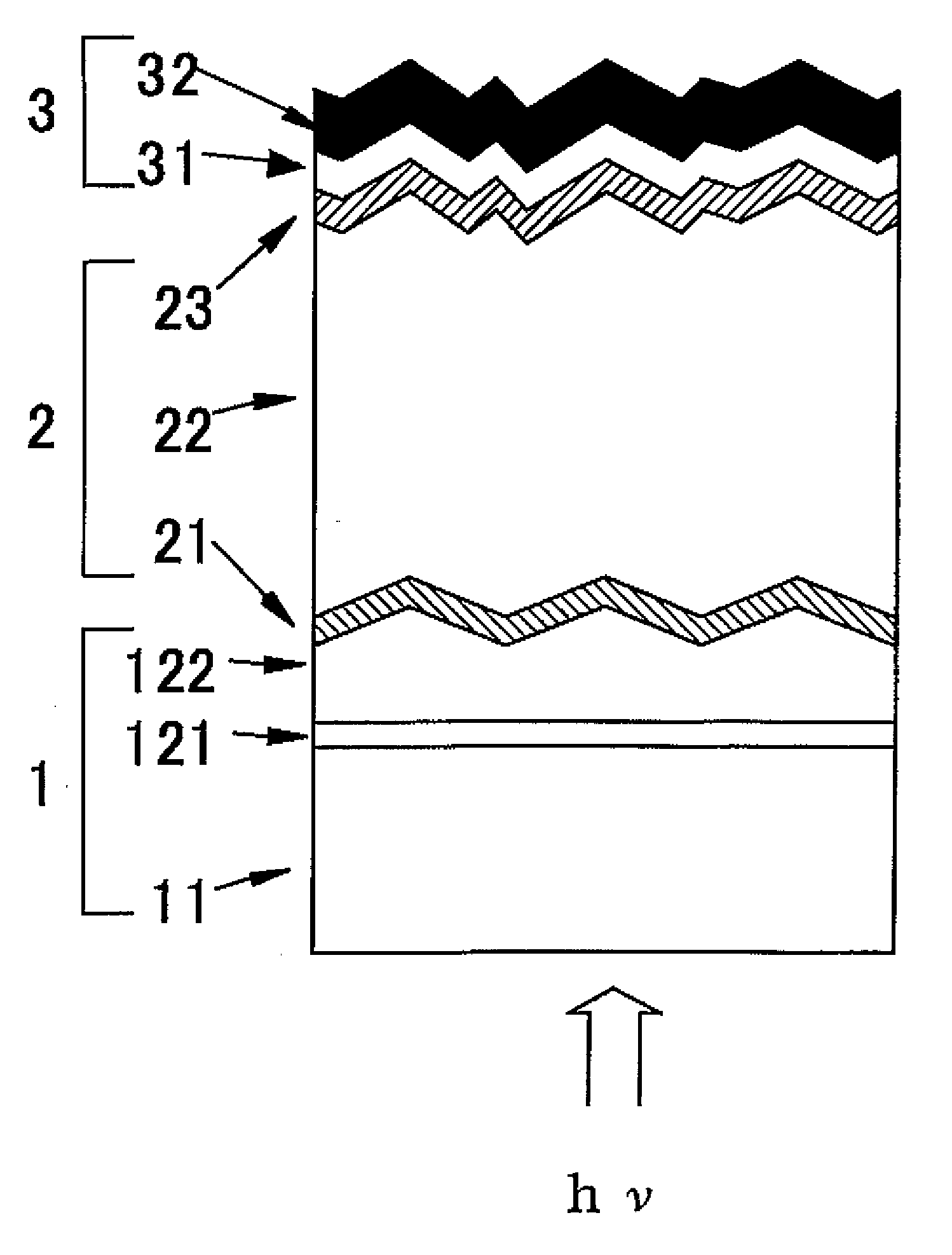
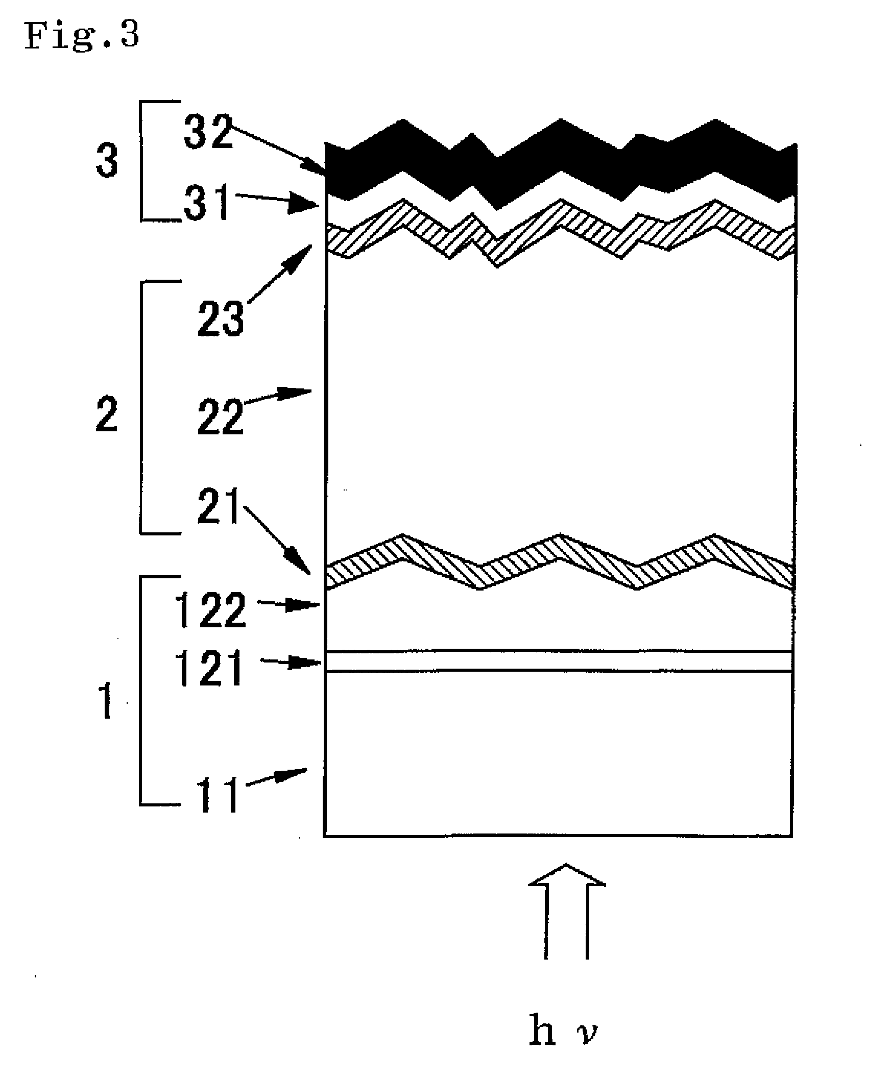
[0057]As Example 1, a substrate 1 provided with a transparent conductive film for a photoelectric conversion device such as shown in FIG. 2 was fabricated.

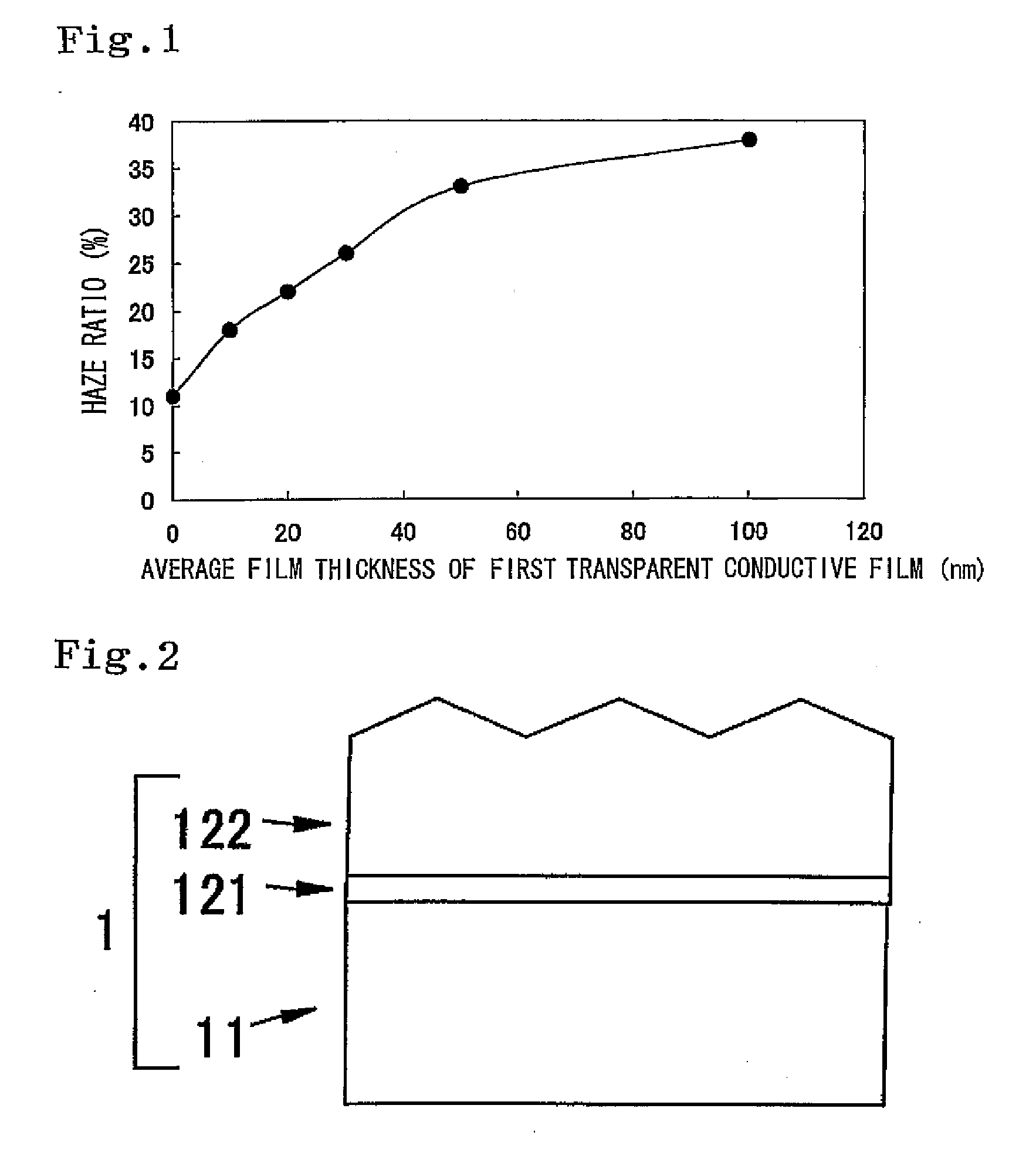
[0058]As the transparent insulating substrate 11, a glass plate having a thickness of 0.7 mm with 125 mm square was used, and Al-doped ZnO was formed to a thickness of 10 nm thereon as the first transparent conductive film 121 by the sputtering method. In forming the first transparent conductive film 121, the substrate temperature was set to be 250° C.; a 3%-Al-doped ZnO with 10-inch (diameter of 254 mm) φ was used as a target; and a condition of the RF power of 400W under an Ar gas atmosphere was used. The haze ratio as measured by the haze meter with use of a D65 light source on the obtained substrate provided with the first transparent conductive film made of the ZnO film was 0.2%. Subsequently, as the second transparent conductive film 122, B-doped ZnO was formed to a thickness of 1.1 μm by the low-pressure CVD method. This se...

example 2

[0060]In Example 2, a substrate 1 provided with a transparent conductive film for a photoelectric conversion device was fabricated in the same manner as in Example 1. However, the difference from Example 1 lies in that the thickness of the first transparent conductive film 121 was set to be 20 nm. The substrate 1 provided with the transparent conductive film for the photoelectric conversion device obtained under this condition had a sheet resistance of about 12 Ω / □ and a haze ratio of 22%. Also, the total light transmittance of the obtained substrate 1 provided with the transparent conductive film for the photoelectric conversion device was measured by allowing light to be incident from the glass plate side with use of a spectrophotometer. It showed a light transmittance of 80% or more within a wavelength range of 400 to 1200 nm.

example 3

[0061]In Example 3, a substrate 1 provided with a transparent conductive film for a photoelectric conversion device was fabricated in the same manner as in Example 1. However, the difference from Example 1 lies in that the thickness of the first transparent conductive film 121 was set to be 30 nm. The substrate 1 provided with the transparent conductive film for the photoelectric conversion device obtained under this condition had a sheet resistance of about 10 Ω / □ and a haze ratio of 26%. Also, the total light transmittance of the obtained substrate 1 provided with the transparent conductive film for the photoelectric conversion device was measured by allowing light to be incident from the glass plate side with use of a spectrophotometer. It showed a light transmittance of 80% or more within a wavelength range of 400 to 1200 nm.


PUM

PropertyMeasurementUnit
Thicknessaaaaaaaaaa
Thicknessaaaaaaaaaa
Thicknessaaaaaaaaaa

Abstract

Provided in this invention is a low-cost substrate provided with a transparent conductive film for photoelectric conversion device, which can improve performance of the photoelectric conversion device by enhanced light confinement effect achieved with effectively increased surface unevenness of the substrate. A method for manufacturing said substrate and a photoelectric conversion device using said substrate which can show improved performance are also provided. The substrate provided with the transparent conductive film for the photoelectric conversion device comprises a transparent insulating substrate and a transparent electrode layer containing at least zinc oxide deposited on the transparent insulating substrate, wherein the transparent electrode layer is composed of a double layer structure wherein first and second transparent conductive films are deposited in this order from a substrate side. The transparent conductive film has an average film thickness of 10-500 nm, and the second transparent conductive film has an average film thickness of 300-1,500 nm. The average film thickness of the second transparent conductive film is larger than that of the first transparent conductive film, and an average height difference of the unevenness on the surface of the second transparent conductive film is 10-300 nm, which is larger than that of the first transparent conductive film.

Description

TECHNICAL FIELD[0001]The present invention relates to a substrate provided with a transparent conductive film for a photoelectric conversion device, a method for manufacturing the substrate, and a photoelectric conversion device using the substrate.BACKGROUND ART[0002]In recent years, in order to make reduction of costs and attainment of higher efficiency be compatible with each other in a solar cell which is one of the photoelectric conversion devices, a thin film solar cell, which can be produced with a small amount of raw materials, is attracting people's attention, and the development is eagerly carried out. In particular, a method of forming a good-quality semiconductor layer on an inexpensive substrate such as glass plate by using a low-temperature process is expected as a method that can realize low costs.[0003]Generally, a thin film solar cell includes a transparent electrode, at least one semiconductor thin film photoelectric conversion unit, and a back electrode that are s...

Claims


Application Information

Patent Timeline
IPC IPC(8): H01L31/042H01L31/00H01L29/45H01L21/283
CPCC23C14/086C23C16/407H01L31/022425Y02E10/50H01L31/0236H01L31/06H01L31/1884H01L31/022466H01L31/02366
Inventor TAWADA, YUKO
Owner KANEKA CORP
Why Eureka
Try Eureka