Organic thin film transistor and organic thin film transistor manufacturing process

a technology of organic thin film transistors and manufacturing processes, which is applied in the field of organic thin film transistors and organic thin film transistor manufacturing processes, can solve the problems of adversely affecting transistor performance, unable to provide source and drain electrodes with high resolution, and unable to achieve high speed and low power consumption. high, good switching property, good stability

Active Publication Date: 2010-02-04
FLEX DISPLAY SOLUTIONS LLC
View PDF5 Cites 9 Cited by
  • Summary
  • Abstract
  • Description
  • Claims
  • Application Information

AI Technical Summary

Benefits of technology

[0023]The present invention can provide an organic thin film transistor with a good switching property and good stability and a process for manufacturing the organic thin film transistor according to a simple method.
[0024]FIG. 1 is a sectional view showing one embodiment of a structure of the organic thin film transistor of the invention.
[0033]10: Light sensitive insulating layer
[0034]Next, preferred embodiments of the invention will be explained in detail.
[0035]In view of the above, extensive study has been made in order to solve the above problems. As a result, the present inventor has found that an organic thin film transistor can be manufactured according to a simple method and can provide good switching property and good stability, which comprises a substrate and provided thereon, at least a source electrode, a drain electrode, an organic semiconductor connecting the source electrode and the drain electrode, a gate electrode, and an insulating layer composed of a plurality of layers, the insulating layer being provided between the gate electrode and the organic semiconductor, wherein the organic thin film transistor comprises a mercapto group-containing compound represented by the following formula (I), and completed the invention.
[0036]Next, the present invention will be explained in detail.

Problems solved by technology

Conventionally, the source electrode, the drain electrode, the gate electrode, the contact electrode or the pixel electrode of an organic thin film transistor has been formed by a vacuum method such as a sputtering method, resulting in cost increase due to the vacuum method.
As a result, it has been found that in the method disclosed in the Patent Document 1, in which a source electrode and a drain electrode are formed via an ink jet method, controlling affinity of ink to a substrate, additives in the ink remain in the electrodes, which adversely affects transistor performance.
It has been also found that the method disclosed in the Patent Document 2, which forms a source electrode and a drain electrode via a screen printing method employing a silver paste, does not provide source and drain electrode with high resolution nor a transistor with high speed and low power consumption.Patent Document 1: Japanese Patent O.P.I. Publication No. 2003-318190Patent Document 2: Japanese Patent O.P.I. Publication No. 2005-72188

Method used


Image

  • Organic thin film transistor and organic thin film transistor manufacturing process
  • Organic thin film transistor and organic thin film transistor manufacturing process
  • Organic thin film transistor and organic thin film transistor manufacturing process

Examples


example 1

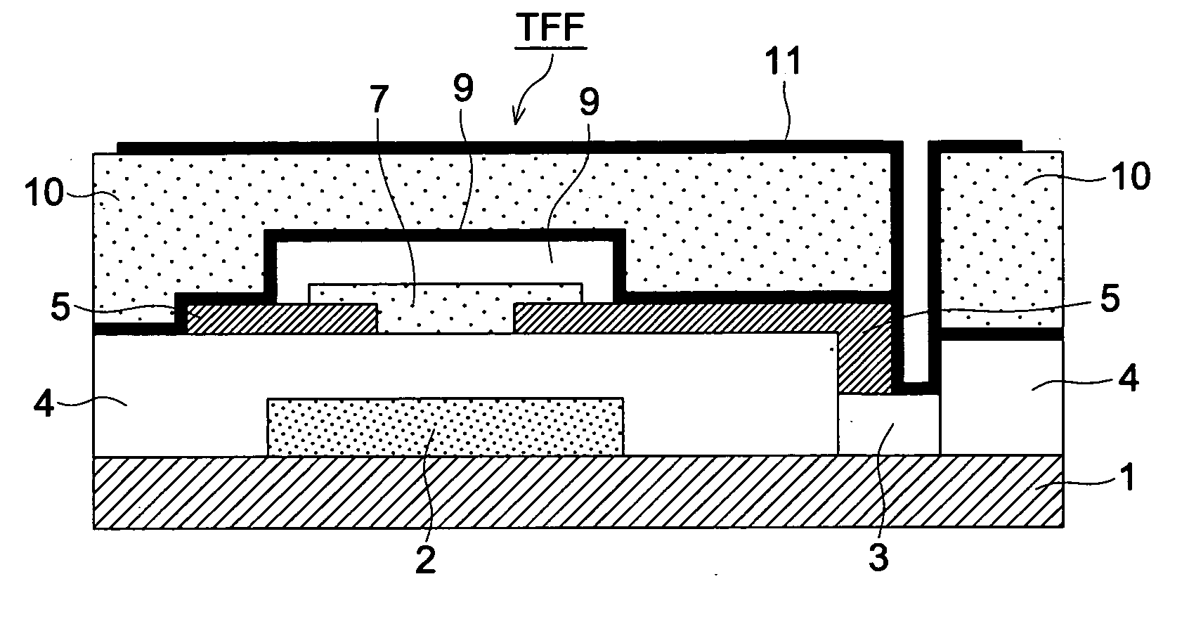
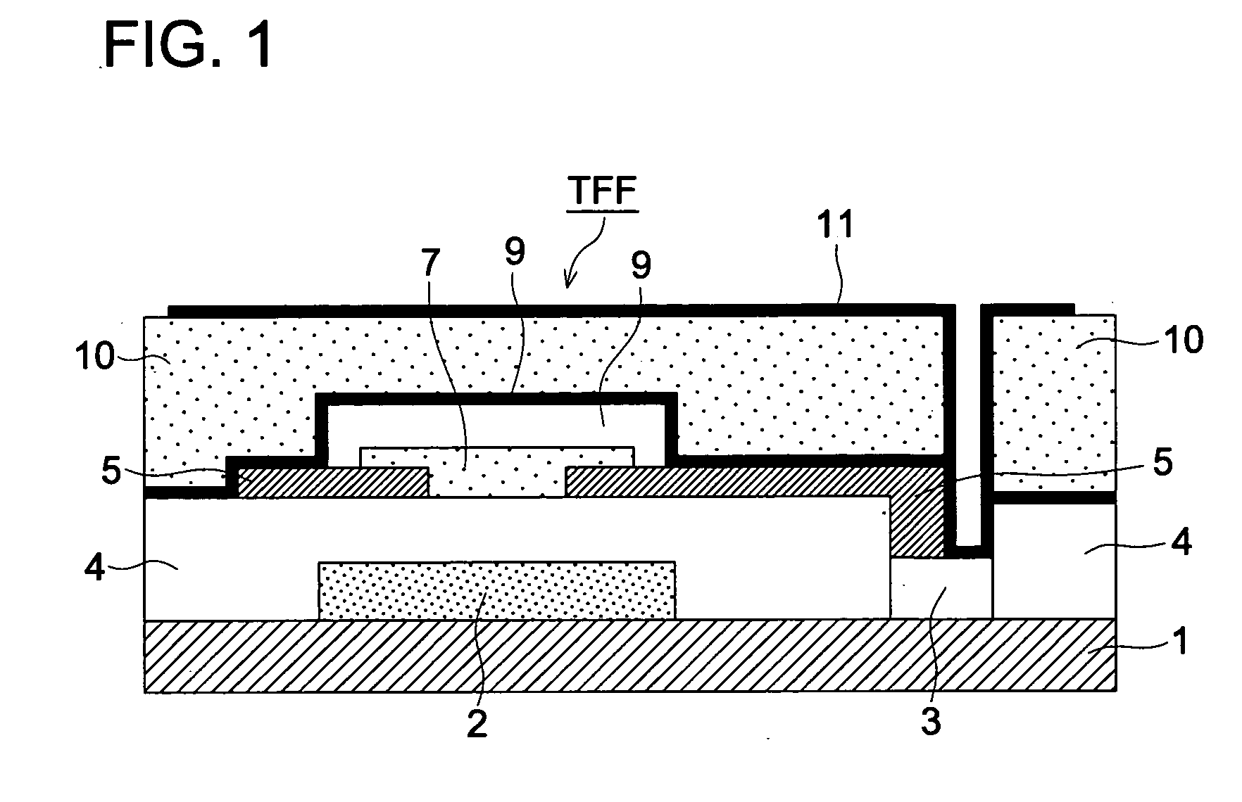
[0093]A layer of an aluminum-neodymium (AlNd) as an aluminum alloy was formed on a glass substrate 1 employing a sputtering method to give a thickness of 150 nm. The AlNd layer was subjected to photolithography treatment and etching treatment to form a gate electrode 2 and a contact electrode 3.

[0094]Subsequently, a SiO2 layer with a thickness of 300 nm was formed employing a plasma CVD method, whereby a gate insulating layer 4 was formed.

[0095]The surface of the resulting gate insulating layer 4 was subjected to UV ozone treatment. The resulting material was immersed in an ethanol solution containing 5 mmol of Exemplified compound (A-2) for 2 hours, and dried at 120° C. for one hour to evaporate the ethanol. The resulting material was exposed to UV light through a mask having an opening at areas where a source electrode and a drain electrode were to be formed, immersed in a Pd catalyst solution, dried, immersed in an electroless gold plating solution, and dried to form a source ele...

example 2

[0102]A glass substrate 1 subjected to a UV / ozone treatment was immersed in an-ethanol solution containing 5 mmol of Exemplified compound (A-1) for 2 hours, and dried at 120° C. for one hour to evaporate ethanol.

[0103]The resulting material was exposed to UV light through a mask having an opening at areas where a gate electrode and a contact electrode are to be formed, immersed in a Pd catalyst solution, dried, immersed in a 0.1 mol / l chromium electroless plating solution, and dried to form a gate electrode 2 and a contact electrode 3 each comprised of chromium according to the mask.

[0104]Subsequently, a SiO2 layer with a thickness of 300 nm was formed employing a plasma CVD method, whereby a gate insulating layer 4 was formed.

[0105]Subsequently, a resist pattern was provided on the insulating layer 4 according to photolithography treatment and etching treatment in order to form a source electrode and a drain electrode according to a lift-off method.

[0106]Subsequently, a chromium la...

example 3

[0113]An aluminum alloy, an aluminum-neodymium (AlNd) layer was formed on a glass substrate 1 employing a sputtering method to give a thickness-of 150 nm. The AlNd layer was subjected to photolithography treatment and etching treatment to form a gate electrode 2 and a contact electrode 3.

[0114]Subsequently, a SiO2 layer with a thickness of 300 nm was formed employing a plasma CVD method, whereby a gate insulating layer 4 was formed.

[0115]Subsequently, a resist pattern was provided on the insulating layer 4 according to photolithography treatment and etching treatment in order to form a source electrode and a drain electrode according to a lift-off method.

[0116]Subsequently, a chromium layer with a thickness of 5 nm was formed on the resist pattern in order to form a source electrode and a drain electrode, and further, a gold layer with a thickness of 50 nm was deposited on the chromium layer according to a sputtering method. Thereafter, the resist pattern was removed with a resist r...


PUM


Abstract

Disclosed is a stable organic thin film transistor having good switching property and a process for manufacturing an organic thin film transistor by a simple method. The organic thin film transistor comprises a substrate and provided thereon, at least a source electrode, a drain electrode, an organic semiconductor connecting the source electrode and the drain electrode, a gate electrode, and an insulating layer composed of a plurality of layers, the insulating layer being provided between the gate electrode and the organic semiconductor, wherein the organic thin film transistor comprises a mercapto group-containing compound represented by the following formula (I),
Formula (I)
(R)n—Si(A)3-n—(B)
wherein R represents an alkyl group having a carbon atom number of not more than 8; A represents an alkoxy group or a halogen atom; B represents a substituent containing an SH group; and n is an integer of from 0 to 2.

Description

FIELD OF THE INVENTION[0001]The present invention relates to a stable organic thin film transistor having a good switching property and an organic thin film transistor manufacturing process.TECHNICAL BACKGROUND[0002]In recent years, an organic thin film transistor (organic TFT, i.e., Organic Thin Film Transistor OTFT) draws attention as a next general flat panel display device with high quality and low price or a switching element for driving pixels of an electronic paper.[0003]An organic thin film transistor has substantially the same structure as a silicon thin film transistor, but is different from a silicon thin film transistor in that it employs an organic substance in the semiconductor active layer. The organic thin film transistor can be manufactured without employing a vacuum apparatus according to an ink jet method or a printing method, and therefore, the organic thin film transistor can be manufactured simply and at low cost as compared with a silicon TFT. The organic thin...

Claims


Application Information

Patent Timeline
Patent Type & Authority Applications(United States)
IPC IPC(8): H01L51/10H01L51/40
CPCB82Y10/00H01L51/0023H01L51/0068H01L51/107H01L51/0525H01L51/0545H01L51/0558H01L51/0094H10K71/621H10K85/655H10K10/472H10K85/40H10K10/484H10K10/88H10K10/466
Inventor HAKII, TAKESHI
Owner FLEX DISPLAY SOLUTIONS LLC
Why Eureka
Try Eureka