

Solar cell and method of manufacturing the same
a solar cell and manufacturing method technology, applied in the field of solar cells, can solve problems such as suppressing the output of solar cells, and achieve the effect of high passivation
- Summary
- Abstract
- Description
- Claims
- Application Information
AI Technical Summary
Benefits of technology
Problems solved by technology
Method used
Image

Examples
example 1
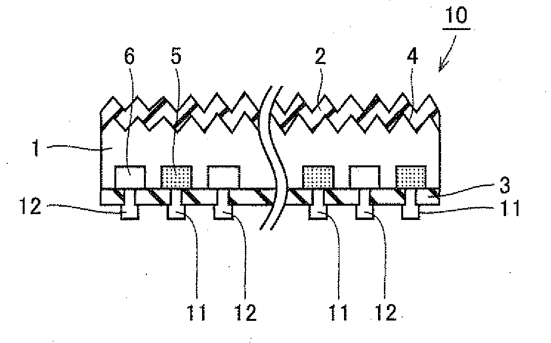
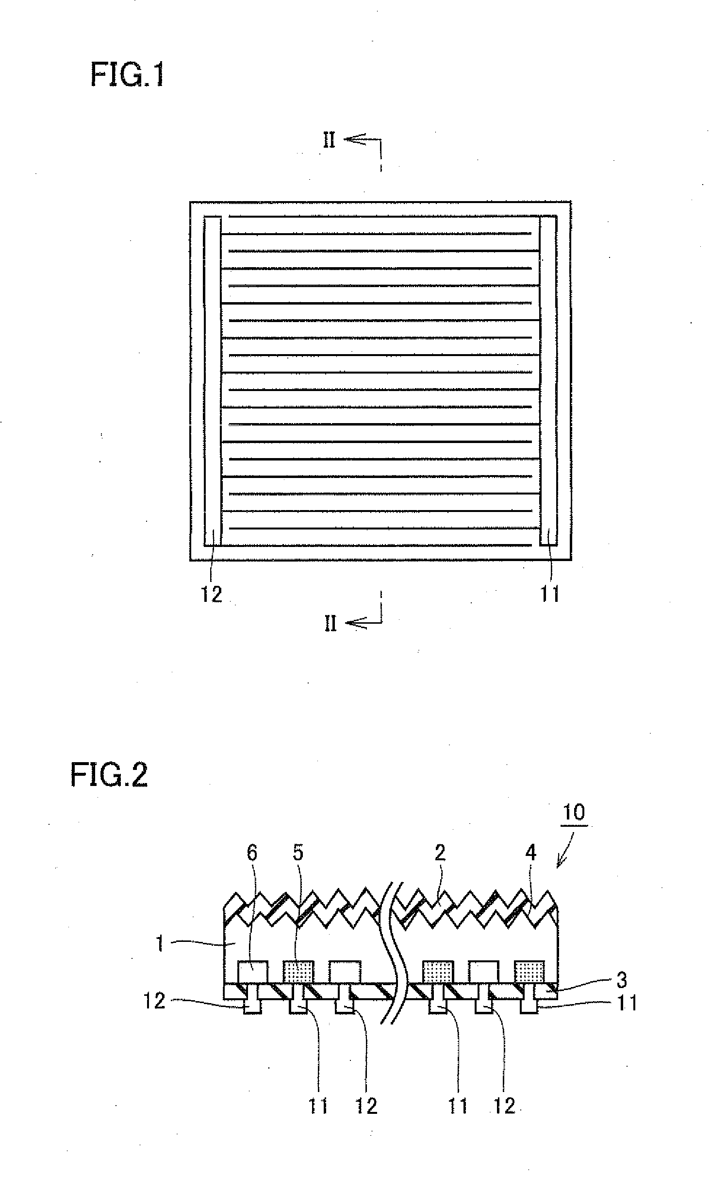
[0073]1: FIG. 5(a)>>
[0074]Firstly, n-type silicon substrate 1 with slice damage caused during slicing removed was prepared. The removal of slice damage from silicon substrate 1 was performed by etching the surface of silicon substrate 1 using sodium hydroxide. As silicon substrate 1, a rectangular silicon substrate with a thickness of 200 μm and a side length of 125 mm was used.
2: FIG. 5(b)>>
[0075]Next, texture mask 7 made of a silicon oxide film was formed on the back surface of silicon substrate 1 by the atmospheric pressure CVD method, and then texture structure 4 was formed on the light-receiving surface of silicon substrate 1. On this occasion, texture mask 7 had a thickness of 800 nm. Texture structure 4 on the light-receiving surface was formed by etching silicon substrate 1 having texture mask 7 formed thereon, using an etching solution. As the etching solution, a solution prepared by adding isopropyl alcohol to potassium hydroxide and heating the mixture to 80° C. was used....
example 2
[0085]A solar cell was fabricated by performing all the steps described in Example 1 except for S7.
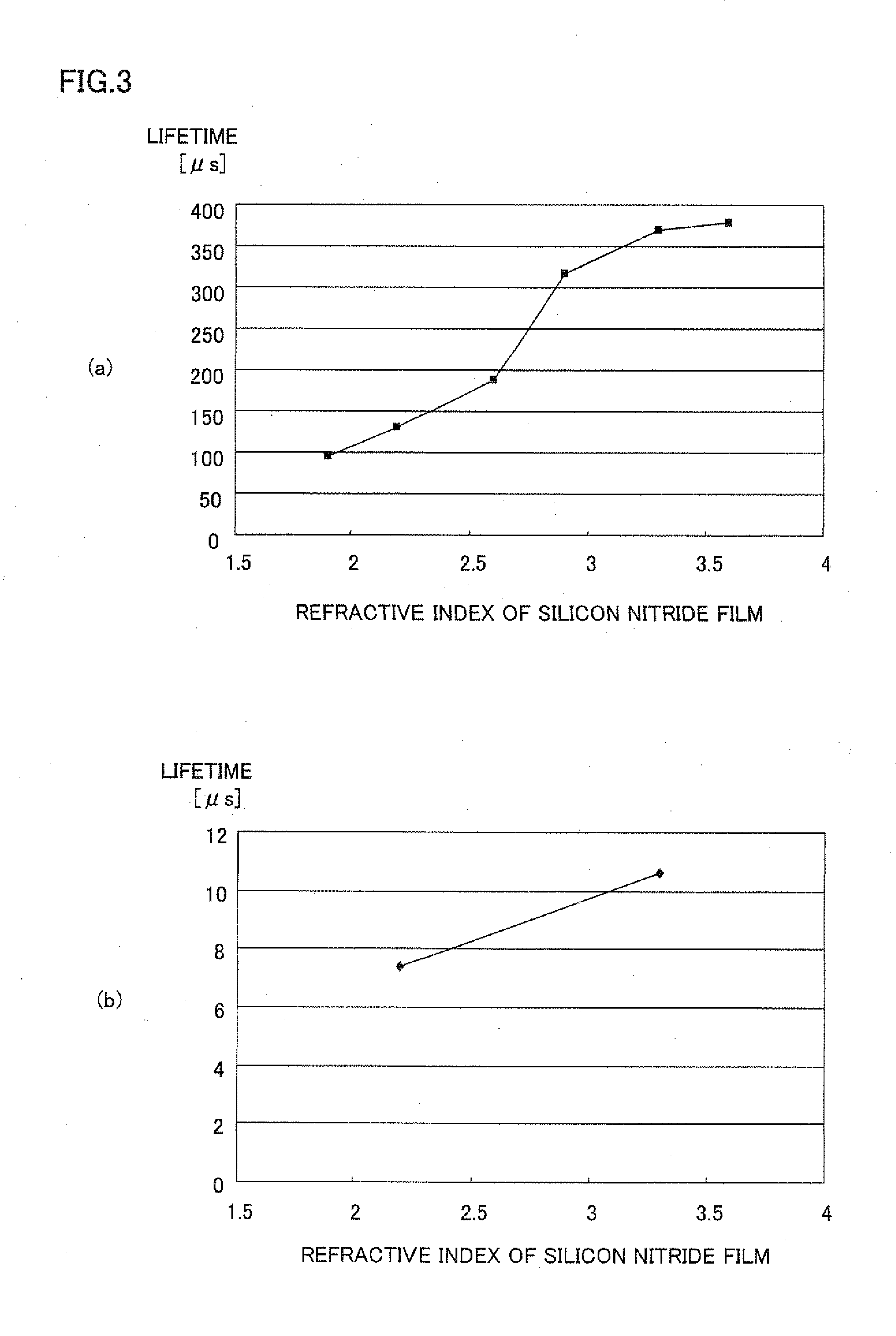
[0086]In the present example, passivation film 3 formed of the first passivation film and the second passivation film made of a silicon oxide film X was employed in S7. Firstly, silicon substrate 1 was treated by the thermal oxidation method at 800° C. for 90 minutes, and thereby a silicon oxide film was formed on each of the light-receiving surface and the back surface of silicon substrate 1. Next, a silicon nitride film with a refractive index of 3.2 was formed by the plasma CVD under the same conditions as those of Example 1. The silicon oxide film on the light-receiving surface was removed by treatment with hydrogen fluoride (i.e., immersing the silicon oxide film in a 2.5% aqueous solution of hydrogen fluoride for 100 seconds). Then, antireflection film 2 made of a silicon nitride film with a refractive index of 2.1 was formed on the light-receiving surface of silicon substrate 1....
PUM
| Property | Measurement | Unit |
|---|---|---|
| refractive index | aaaaa | aaaaa |
| thickness | aaaaa | aaaaa |
| thickness | aaaaa | aaaaa |
Abstract
Description
Claims
Application Information