Surface preparation process for damascene copper deposition

a preparation process and damascene technology, applied in the direction of basic electric elements, semiconductor/solid-state device manufacturing, electric devices, etc., can solve the problems of tantalum nitride being negative, affecting the electrical characteristics of the electrodes, and poor adhesion of the copper layer deposited thereon

Active Publication Date: 2010-03-25
MACDERMID ENTHONE INC
View PDF21 Cites 41 Cited by
  • Summary
  • Abstract
  • Description
  • Claims
  • Application Information

AI Technical Summary

Benefits of technology

[0009]Briefly, the present invention is directed to a method of metallizing a substrate comprising an interconnect feature in the manufacture of a microelectronic device, wherein the interconnect feature comprises a bottom, a sidewall, and a top opening having a diameter, D. The method comprises depositing a barrier layer on the bottom and the sidewall of the interconnect feature, the barrier layer comprising a metal selected from the group consisting of ruthenium, tungsten, tantalum, titanium, iridium, rhodium, and combinations thereof; contacting the substrate comprising the interconnect feature comprising the bottom and sidewall having the barrier layer thereon with an aqueous composition comprising a reducing agent; and depositing copper metal onto the bottom and the sidewall of the interconnect feature having the barrier layer thereon.

Problems solved by technology

The barrier layer is deposited since copper has a tendency to diffuse into the semiconductor's junctions, thereby disturbing their electrical characteristics.
Tantalum nitride has negative characteristics, which include poor adhesion to the copper layer deposited thereon.
Poor adhesion of the subsequently deposited copper layers can lead to poor electromigration in the formed device and possibly cause process contamination issues in subsequent processing steps, such as during a chemical mechanical polishing (CMP) process.
However, adhesion of copper deposits through direct electrochemical plating processes on those resistive barriers other than ruthenium is an issue.
Although ruthenium is a fairly conductive material, its sheet resistance at nano-scale thickness is still too high to be electrolytically plated uniformly.
Global uniformity of electrolytic copper deposition (ECP) on ruthenium is currently unacceptable due to significant degree of terminal effect.

Method used


Image

  • Surface preparation process for damascene copper deposition
  • Surface preparation process for damascene copper deposition
  • Surface preparation process for damascene copper deposition

Examples


example 1

Pre-Treatment Composition

[0074]A pre-treatment composition was prepared to contain the following components and approximate concentrations:

[0075]Dimethylamine Borane (100 g / L)

[0076]CALFOAM® EA-603 (100 g / L)

[0077]Balance water 1 liter.

example 2

Pre-Treatment Composition

[0078]A pre-treatment composition was prepared to contain the following components and approximate concentrations:

[0079]Hypophosphorous acid (20 g / L)

[0080]Dimethyl amine Borane (2 g / L)

[0081]Diethylamine (20 g / L)

[0082]Balance water 1 liter.

example 3

Study of Induction Time of Electroless Copper Deposition on Various Seed Layers

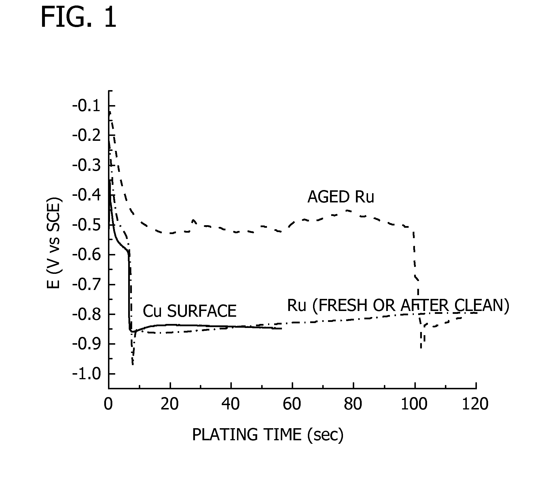
[0083]The induction time of electroless copper deposition on ruthenium seed layers treated with the composition of Example 1 were measured using open-circuit potential change with time using a potentiostat and Standard Calomel Electrode (SCE) on blanket substrates.

[0084]FIG. 1 is a graph showing the induction time of electroless copper deposition on ruthenium substrates (freshly prepared and aged) compared to that on a PVD copper substrate. Electroless copper deposition was rapidly initiated on freshly prepared ruthenium substrates and on the copper surface. A ruthenium surface aged for 9 months in air (humidity was not controlled) exhibited delay deposition initiation (over 100 seconds), which is thought to be due to oxidation of the ruthenium surface. In some cases, electroless copper deposition did not initiate on aged ruthenium surfaces.

[0085]The aged ruthenium substrate was pre-treated prior to elect...


PUM

PropertyMeasurementUnit
widthaaaaaaaaaa
widthaaaaaaaaaa
lengthaaaaaaaaaa

Abstract

A method is disclosed for metallizing a substrate comprising an interconnect feature in the manufacture of a microelectronic device, wherein the interconnect feature comprises a bottom, a sidewall, and a top opening having a diameter, D. The method comprises the following steps: depositing a barrier layer on the bottom and the sidewall of the interconnect feature, the barrier layer comprising a metal selected from the group consisting of ruthenium, tungsten, tantalum, titanium, iridium, rhodium, and combinations thereof; contacting the substrate comprising the interconnect feature comprising the bottom and sidewall having the barrier layer thereon with an aqueous composition comprising a reducing agent and a surfactant; and depositing copper metal onto the bottom and the sidewall of the interconnect feature having the barrier layer thereon.

Description

FIELD OF THE INVENTION[0001]The present invention generally relates to a process for preparing the surface of a barrier layer and / or liner material for subsequent copper deposition in the manufacture of microelectronic devices.BACKGROUND OF THE INVENTION[0002]The demand for semiconductor integrated circuit (IC) devices such as computer chips with high circuit speed and high circuit density requires the downward scaling of feature sizes in ultra-large scale integration (ULSI) and very-large scale integration (VLSI) structures. The trend to smaller device sizes and increased circuit density requires decreasing the dimensions of interconnect features and increasing their density. An interconnect feature is a feature such as a trench or via formed in a dielectric substrate which is then filled with metal to yield an electrically conductive interconnect. Copper, having better conductivity than any metal except silver, is the metal of choice since copper metallization allows for smaller f...

Claims


Application Information

Patent Timeline
Patent Type & Authority Applications(United States)
IPC IPC(8): H01L21/768
CPCH01L21/02068H01L21/288H01L21/76843H01L21/76874H01L21/76861H01L21/76873H01L21/76846
Inventor CHEN, QINGYUNLIN, XUANPANECCASIO, JR., VINCENTHURTUBISE, RICHARD
Owner MACDERMID ENTHONE INC
Why Eureka
Try Eureka