Method for Fabricating Organic Optoelectronic Multi-Layer Devices

a multi-layer device and optoelectronic technology, applied in the field of optoelectronics, can solve the problems of inability to fabricate arbitrary, all-solution-processed multi-layer polymer electronics, and the performance of inorganic based devices is comparatively lower than that of inorganic based devices, so as to improve the quality of polymer film fabrication, reduce cost, flexibility, and reduce weight

Inactive Publication Date: 2010-04-08
ACAD SINIC
View PDF10 Cites 2 Cited by
  • Summary
  • Abstract
  • Description
  • Claims
  • Application Information

AI Technical Summary

Benefits of technology

[0013]Disclosed is a method that provides a way to universally improve polymer film fabrication via a polydimethylsiloxane (PDMS) transferring process. In comparison to traditional inorganic optoelectronics, organic based optoelectronics offer unique advantages, such as reduced cost, flexibility, reduced weight, and an improved eco-process. A cascade architecture layer is constructed layer-by-layer via a PDMS polymer thin-film transference. The method eliminates the need for any unwanted molecules and the damage that they can potentially cause on bottom films, which results from the preceding film during the transfer process. As a result, a stable, fast and reproducible way is achieved to fabricate organic optoelectronic multi-layer devices.
[0014]The method comprises initially treating the surface of a PDMS stamp with at least one organic solvent, such as acetone, toluene or cholorobenzene, based on the solvent used for the polymer solution. Here, the organic solvents not only clean the PDMS surface, but also eliminate any stress on the PDMS surface caused by the stamp formation process. More importantly, however, the homogeneity of the polymer film around the PDMS surface must be maintained by residual solvent vapor.
[0016]A modified printing method is provided that increases the affinity of PDMS for organic solvents via a non-destructive solvent treatment. The disclosed method eliminates the necessity for a plasma treatment, and any possible damage to the PDMS surface such that full control over the chemical composition and film thickness of each layer is provided.
[0017]The method permits improvement of the efficiency of organic optoelectronics, as well as diversification of the fabrication of organic optoelectronics. The disclosed method surpasses inorganic optoelectronics by permitting the further development of high efficiency organic materials. The disclosed method is implemented in a non-vacuum environment, and the multi-layer structure can be achieved by transferring the polymer from the PDMS stamp. The method eliminates the necessity to include an extra supporting layer for film transfers from the PDMS surface to the target surface. As a result, PDMS stamps are achieved that can be reused for tens of layers. The method also permits the easy formation of a large coverage area having a uniform polymer film on the PDMS stamp surface. Moreover, an optimum contact between the preceding layer and the successive layer can be achieved. In addition, it becomes possible to fabricate the uniform polymer film on top of the PDMS stamp without any extra treatment of the PDMS stamp, such as UV-ozone and plasma treatments. The multilayer polymer structure also has use in photovoltaic applications.

Problems solved by technology

The performance of these devices is comparatively lower than that of inorganic based devices due to limitations associated with optical absorption and the migration of strongly bound photo generated excitons.
However, there are problems encountered by the conventional spin coating process for polymer materials, which need to be solved for such multilayer structures because of the dissolution of the previous layer by an organic solvent.
At present, there is no widespread and reliable method with which to fabricate arbitrary, all-solution-processed multilayer polymer electronics.
Considerable progress has been made in designing solution-processed organic semiconductors; however, the performance of the devices is somehow restricted by their relatively poor carrier transfer properties and large energy bandgaps, which result in poor performance compared to most of their inorganic counterparts.
However, dissolution of the initial layer by the subsequent layers during spin coating acts as a barrier to the realization of multilayer spin coating films.
A drawback associated with the use of cross-linking polymers is that the performance of the polymers is decreased after the cross-linking process.
A disadvantage associated with the use of different solvents is that only a limited combination of materials and solvents can be chosen.
However, unwanted molecules used for transferring the polymer films from the silicon wafer to the PDMS contaminate the original device materials.
As a result, a decrease in the performance of the device occurs.
Although this method prevents the dissolution problem, this method is overly complex and the residual of the sacrificial layer contaminates the interface between two organic layers, resulting in a decrease in device performance.
However, this destructive physical treatment procedure not only complicates the entire process but also causes extensive damage to the surface structure of the PDMS due to the high power plasma treatment.
Consequently, the morphology of the transferred polymer films is influenced, which leads to poor solar cell performance.

Method used


Image

  • Method for Fabricating Organic Optoelectronic Multi-Layer Devices
  • Method for Fabricating Organic Optoelectronic Multi-Layer Devices
  • Method for Fabricating Organic Optoelectronic Multi-Layer Devices

Examples


Embodiment Construction

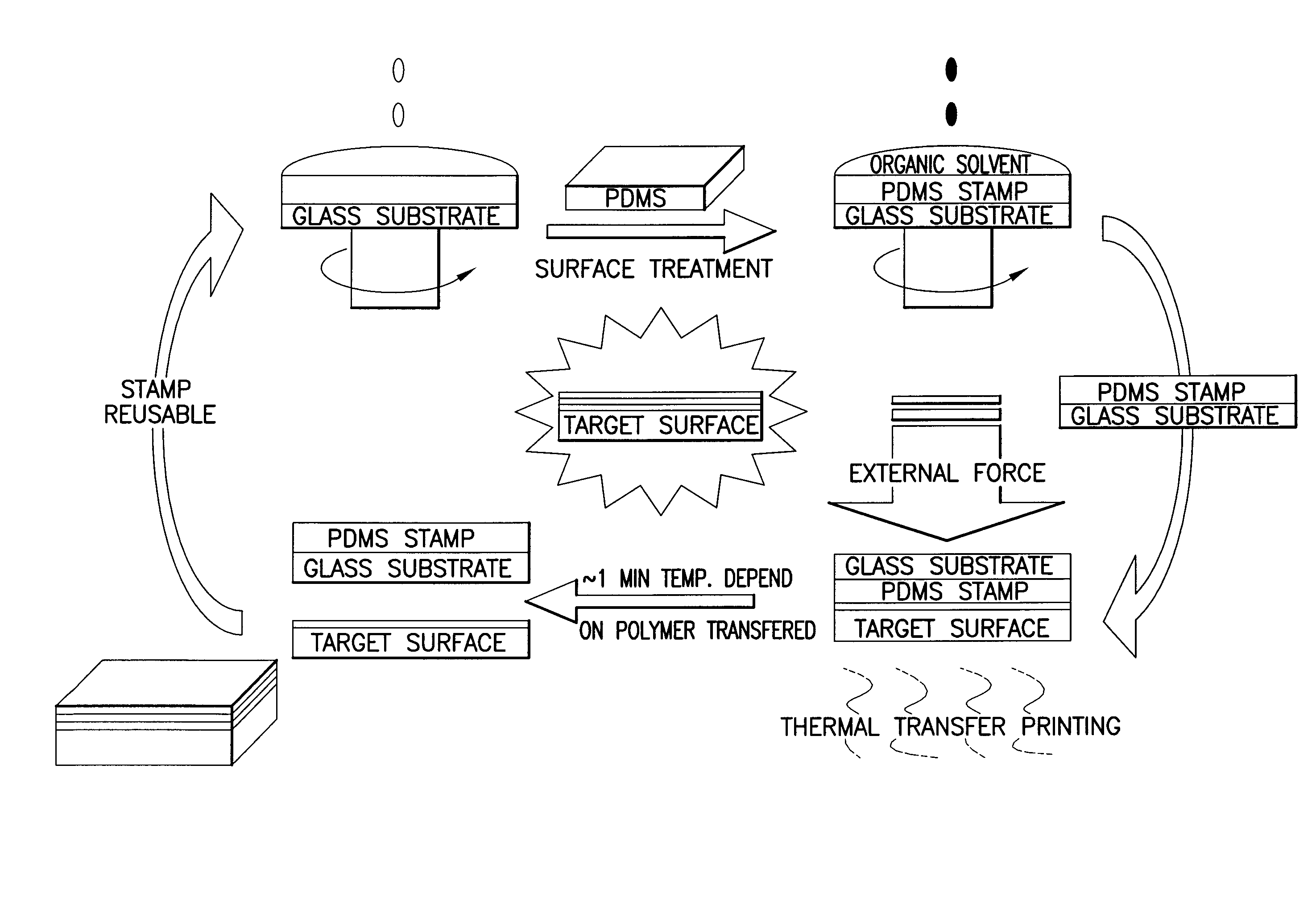
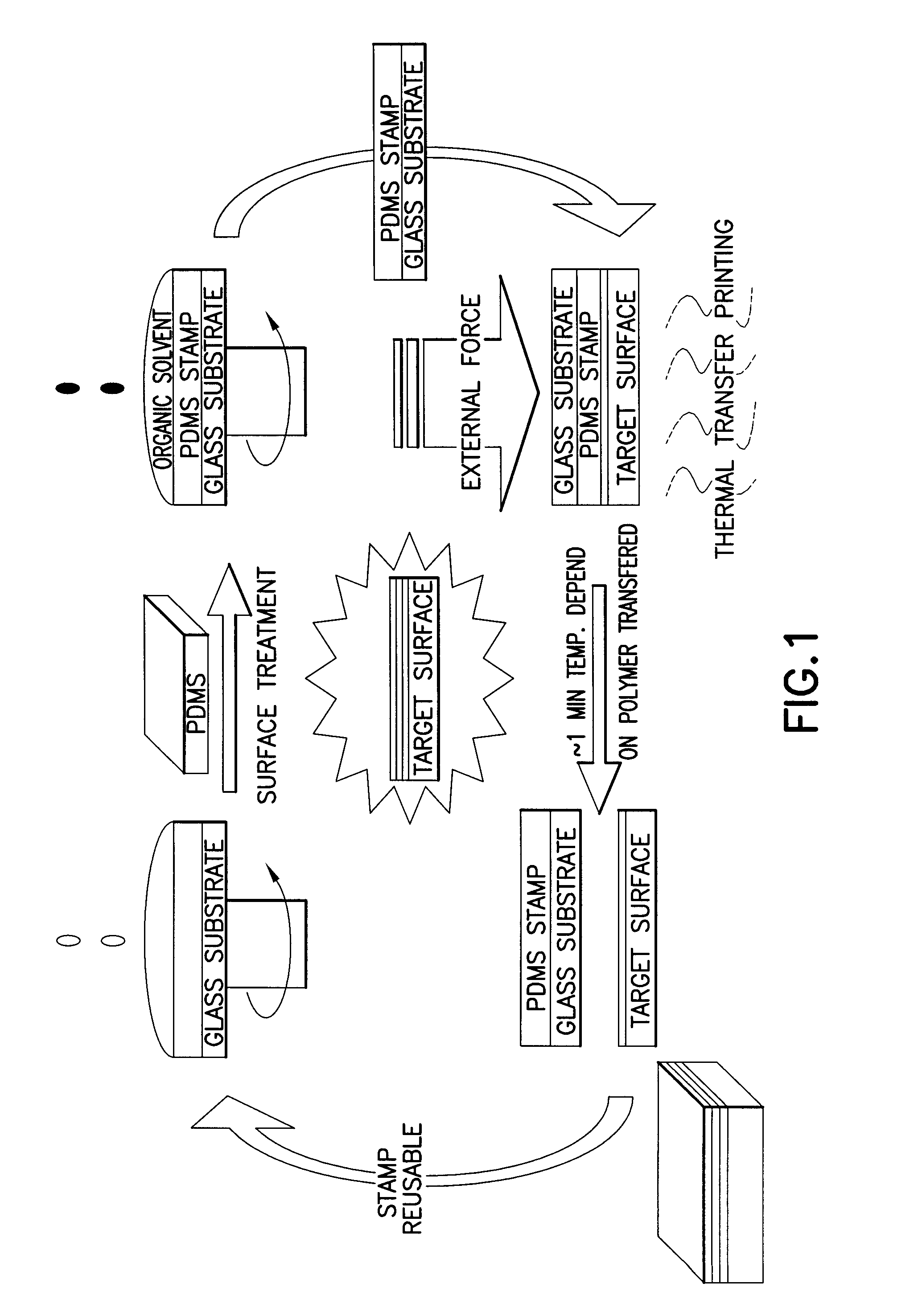
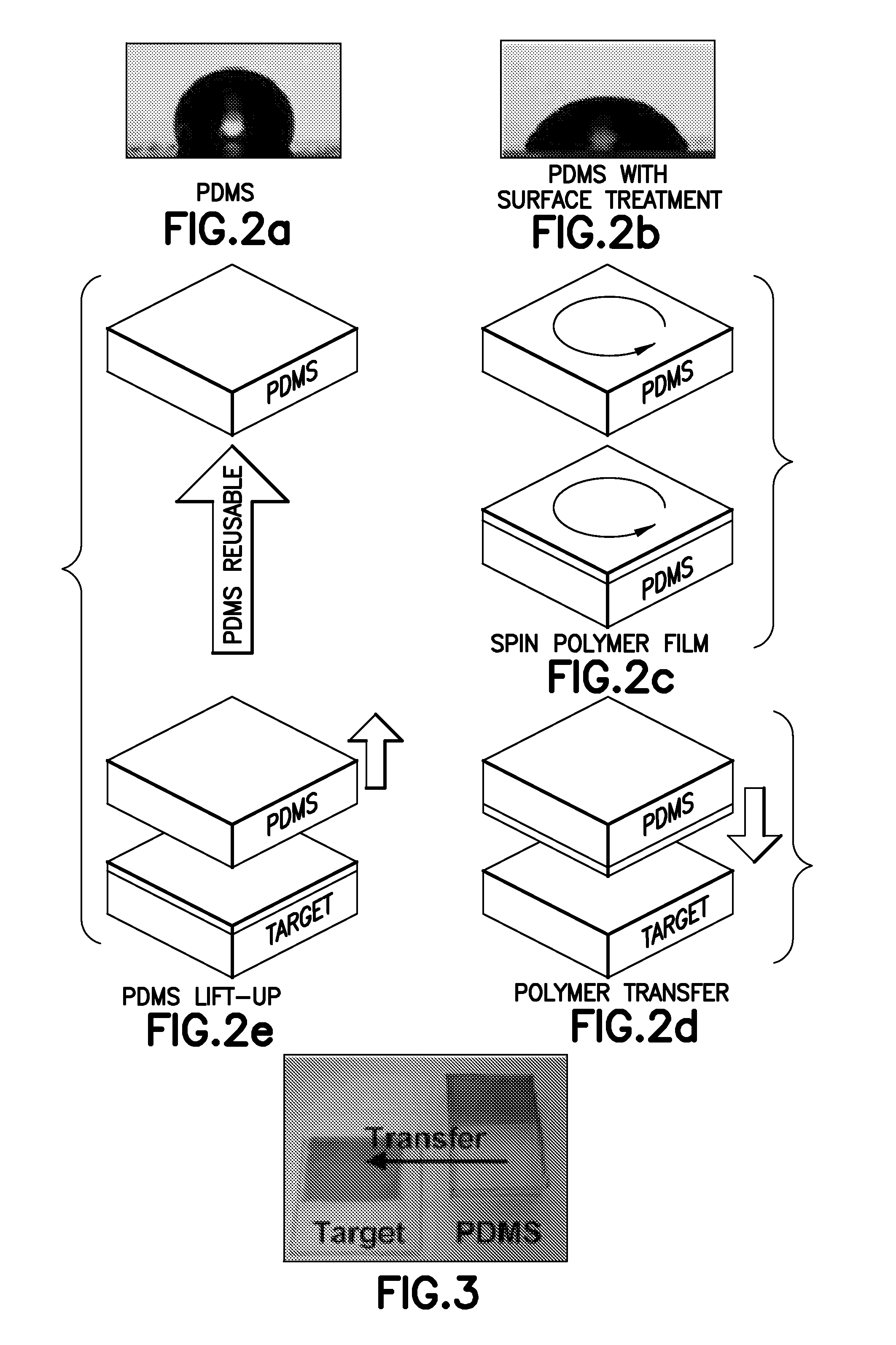
[0035]Disclosed is a method that provides a way to universally improve polymer film fabrication via a polydimethylsiloxane (PDMS) transferring process. A cascade architecture layer is constructed layer-by-layer via a PDMS polymer thin-film transference. The method eliminates the need for any unwanted molecules and the damage that they can potentially cause on bottom films, which results from the preceding film during the transferring process. As a result, a stable, fast and reproducible way is achieved to fabricate organic optoelectronic multi-layer devices.

[0036]FIG. 1 is a flow diagram of a film transfer in accordance with the method of the invention. In general, the method comprises treating a PDMS surface comprising a silicon wafer fixed on a glass substrate with organic solvents by spinning. Next, the transferred film from an organic solvent is spun directly on the PDMS stamp. An external force and thermal annealing are simultaneously used to transfer the film spun on the PDMS ...


PUM

PropertyMeasurementUnit
temperatureaaaaaaaaaa
shear stressaaaaaaaaaa
pressureaaaaaaaaaa

Abstract

A method for fabricating organic optoelectronics multi-layer devices is disclosed. A polydimethylsiloxane (PDMS) surface is pretreated with an organic solvent and used to directly form a uniform optoelectrical thin-film from organic solution by spin coating. The optoelectrical thin-film films that are formed on the PDMS surface are easily transferable to any substrate by a slight, externally applied force for providing conformal contact with a target substrate and thermal annealing, depending on the polymers to be transferred. Pretreatment of the PDMS surface with the organic solvent combined with a dry transfer process provides an easier way to cascade polymer architecture fabrication. In addition, the method increases the performance of various types of organic photo electronics, and permits an extension of the types of research that can be performed in the field of photo electronics.

Description

CROSS-REFERENCE TO RELATED APPLICATIONS[0001]This application claims priority from U.S. Provisional Application Ser. No. 61 / 188,065 filed Aug. 6, 2008, the content of which is hereby incorporated by reference in its entirety.BACKGROUND OF THE INVENTION[0002]1. Field of the Invention[0003]The present invention generally relates to the field of optoelectronics and, more particularly, to a method for fabricating organic optoelectronics multi-layer devices.[0004]2. Description of the Related Art[0005]A considerable level of research in organic thin-film electronics has led to the creation of devices, such as organic transistors, solar cells and light emitting diodes. The performance of these devices is comparatively lower than that of inorganic based devices due to limitations associated with optical absorption and the migration of strongly bound photo generated excitons. However, organic electronics still provide an advantage with respect to cost of fabrication, flexible substrates, re...

Claims


Application Information

Patent Timeline
Patent Type & Authority Applications(United States)
IPC IPC(8): B32B37/02
CPCB32B37/025B32B2309/02B32B2309/04B32B2457/206B32B2315/08B32B2367/00B32B2309/105
Inventor CHU, CHIH-WEIHO, ZHONG-YO
Owner ACAD SINIC
Why Eureka
Try Eureka