Semiconductor device and method for manufacturing the same

a technology of semiconductors and semiconductors, applied in the direction of transistors, electroluminescent light sources, electric lighting sources, etc., can solve the problems of increased manufacturing costs, and achieve the effect of reducing manufacturing costs and improving reliability of thin film transistors

Active Publication Date: 2010-04-29
SEMICON ENERGY LAB CO LTD
View PDF100 Cites 300 Cited by
  • Summary
  • Abstract
  • Description
  • Claims
  • Application Information

AI Technical Summary

Benefits of technology

[0033]By forming the thin film transistor using the oxide semiconductor interposed between the two gate electrodes provided above and below the oxide semiconductor in a peripheral circuit such as a gate line driver circuit or a source line driver circuit, or a pixel portion, manufacturing cost is reduced.
[0034]With the thin film transistor using the oxide semiconductor interposed between the two gate electrode

Problems solved by technology

When the number of the gate lines and the signal lines is increased, it is difficult to mount IC chips including driver ci

Method used


Image

  • Semiconductor device and method for manufacturing the same
  • Semiconductor device and method for manufacturing the same
  • Semiconductor device and method for manufacturing the same

Examples


embodiment 1

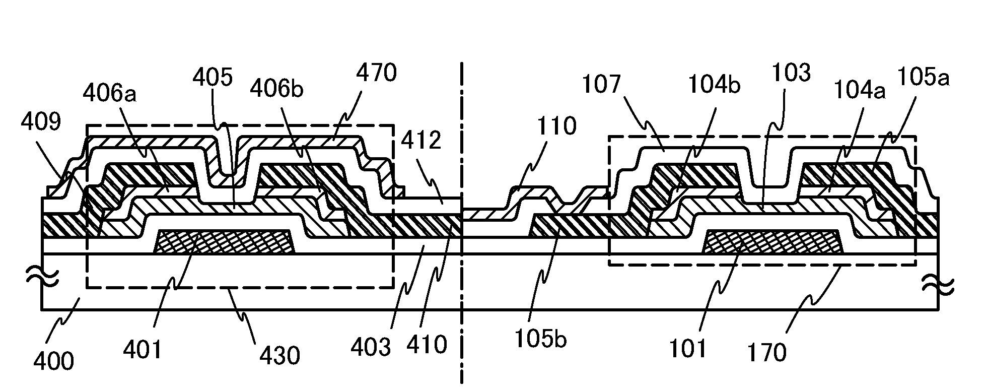
[0063]FIG. 1A illustrates an example in which a first thin film transistor 430 used for a driver circuit and a second thin film transistor 170 used for a pixel portion are provided over the same substrate. Note that FIG. 1A is also an example of a cross-sectional view of a display device.

[0064]The pixel portion and the driver circuit are formed over the same substrate. In the pixel portion, the second thin film transistors 170, which are enhancement type transistors, arranged in a matrix form are each used for switching on / off of voltage application to a pixel electrode 110. The second thin film transistor 170 arranged in the pixel portion is formed using an oxide semiconductor layer 103. As for electric characteristics of the second thin film transistor, on / off ratio is 109 or more at a gate voltage ±20 V; therefore, display contrast can be improved, and further, leakage current is small, whereby low power consumption driving can be realized. The on / off ratio is a ratio of on curre...

embodiment 2

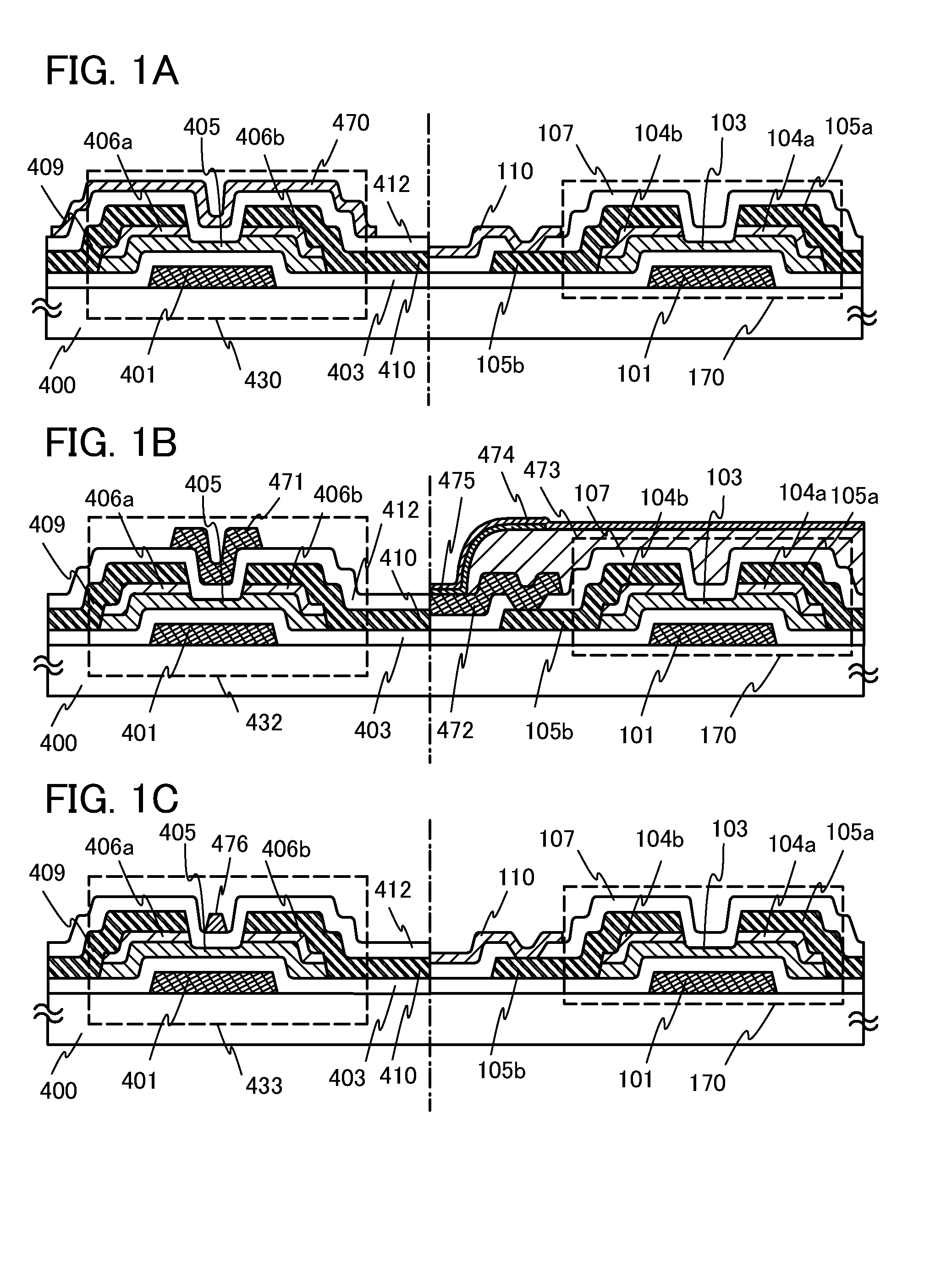
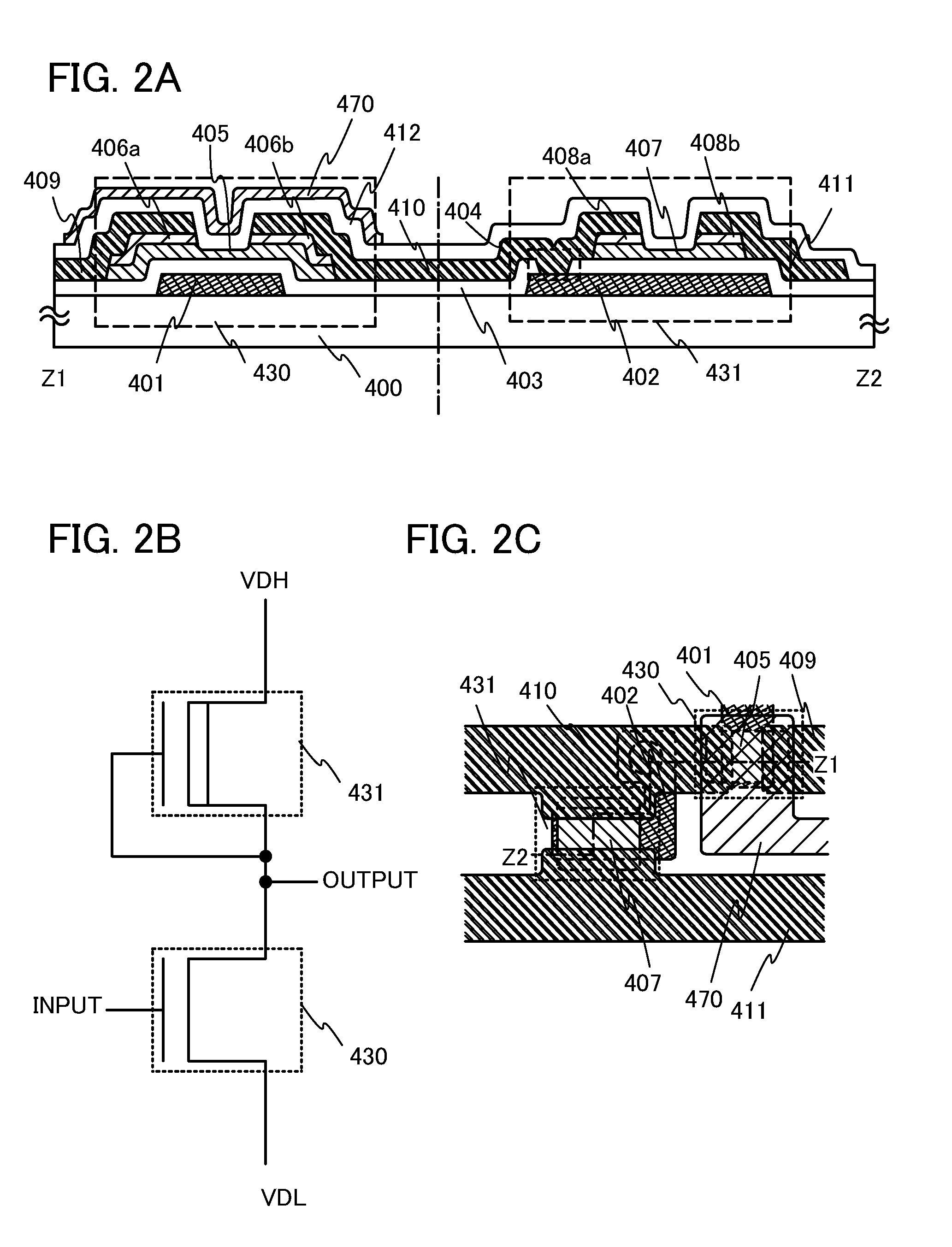
[0080]Although one thin film transistor has been described as the thin film transistor in the driver circuit in Embodiment 1, an example of forming an inverter circuit of a driver circuit with use of two n-channel thin film transistors will be described below in Embodiment 2. A thin film transistor illustrated in FIG. 2A is the same as the thin film transistor 430 illustrated in FIG. 1A of Embodiment 1; therefore, the same parts are denoted by the same reference numerals.

[0081]The driver circuit for driving a pixel portion is formed using an inverter circuit, a capacitor, a resistor, and the like. When the inverter circuit is formed using two n-channel TFTs in combination, there are an inverter circuit having a combination of an enhancement type transistor and a depletion type transistor (hereinafter, referred to as an EDMOS circuit) and an inverter circuit having a combination of two enhancement type TFTs (hereinafter, referred to as an EEMOS circuit).

[0082]A cross-sectional struct...

embodiment 3

[0096]In Embodiment 3, a display device will be described with reference to block diagrams and the like.

[0097]FIG. 3A illustrates an example of a block diagram of an active matrix liquid crystal display device. The liquid crystal display device illustrated in FIG. 3A includes, over a substrate 300, a pixel portion 301 having a plurality of pixels each provided with a display element; a scan line driver circuit 302 which controls a scan line connected to a gate electrode of each pixel; and a signal line driver circuit 303 which controls video signal input to a selected pixel.

[0098]FIG. 3B illustrates an example of a block diagram of an active matrix light-emitting display device. The light-emitting display device illustrated in FIG. 3B includes, over a substrate 310, a pixel portion 311 having a plurality of pixels each provided with a display element; a first scan line driver circuit 312 and a second scan line driver circuit 313, each of which controls a scan line connected to a gat...


PUM


Abstract

As a display device has a higher definition, the number of pixels, gate lines, and signal lines are increased. When the number of the gate lines and the signal lines are increased, a problem of higher manufacturing cost, because it is difficult to mount an IC chip including a driver circuit for driving of the gate and signal lines by bonding or the like. A pixel portion and a driver circuit for driving the pixel portion are provided over the same substrate, and at least part of the driver circuit includes a thin film transistor using an oxide semiconductor interposed between gate electrodes provided above and below the oxide semiconductor. Therefore, when the pixel portion and the driver portion are provided over the same substrate, manufacturing cost can be reduced.

Description

TECHNICAL FIELD[0001]The present invention relates to a semiconductor device using an oxide semiconductor and a method for manufacturing the semiconductor device.BACKGROUND ART[0002]A thin film transistor formed over a flat plate such as a glass substrate is manufactured using amorphous silicon or polycrystalline silicon, as typically seen in a liquid crystal display device. A thin film transistor formed using amorphous silicon has low electric field effect mobility, but such a transistor can be formed over a glass substrate with a larger area. On the other hand, a thin film transistor formed using crystalline silicon has high electric field effect mobility, but a crystallization process such as laser annealing is necessary and such a transistor is not always suitable for a larger glass substrate.[0003]In view of the foregoing, attention has been drawn to a technique by which a thin film transistor is formed using an oxide semiconductor, and such a transistor is applied to an electr...

Claims


Application Information

Patent Timeline
IPC IPC(8): H01L33/00H01L29/786H05B44/00
CPCH01L27/1225H01L27/1251H01L29/7869H01L29/78648H01L29/78621H01L27/124H01L29/786H01L21/477H01L27/1259H01L29/24H01L29/41733H01L29/42384H01L29/66969H01L29/78645H01L21/02565H01L21/47635H01L29/42356H01L29/45
Inventor MIYAIRI, HIDEKAZUOSADA, TAKESHIYAMAZAKI, SHUNPEI
Owner SEMICON ENERGY LAB CO LTD
Why Eureka
Try Eureka