Method for producing piezoelectric composite substrate

a composite substrate and piezoelectric technology, applied in the field of piezoelectric composite substrate production, can solve the problems of difficult cutting and low efficiency of microcavity formation

Active Publication Date: 2010-05-06
MURATA MFG CO LTD
View PDF6 Cites 26 Cited by
  • Summary
  • Abstract
  • Description
  • Claims
  • Application Information

AI Technical Summary

Benefits of technology

[0009]To overcome the problems described above, preferred embodiments of the present invention provide a method fo

Problems solved by technology

With hydrogen ions, the bonds are difficult to cut because hydrogen has a l

Method used


Image

  • Method for producing piezoelectric composite substrate
  • Method for producing piezoelectric composite substrate
  • Method for producing piezoelectric composite substrate

Examples


Embodiment Construction

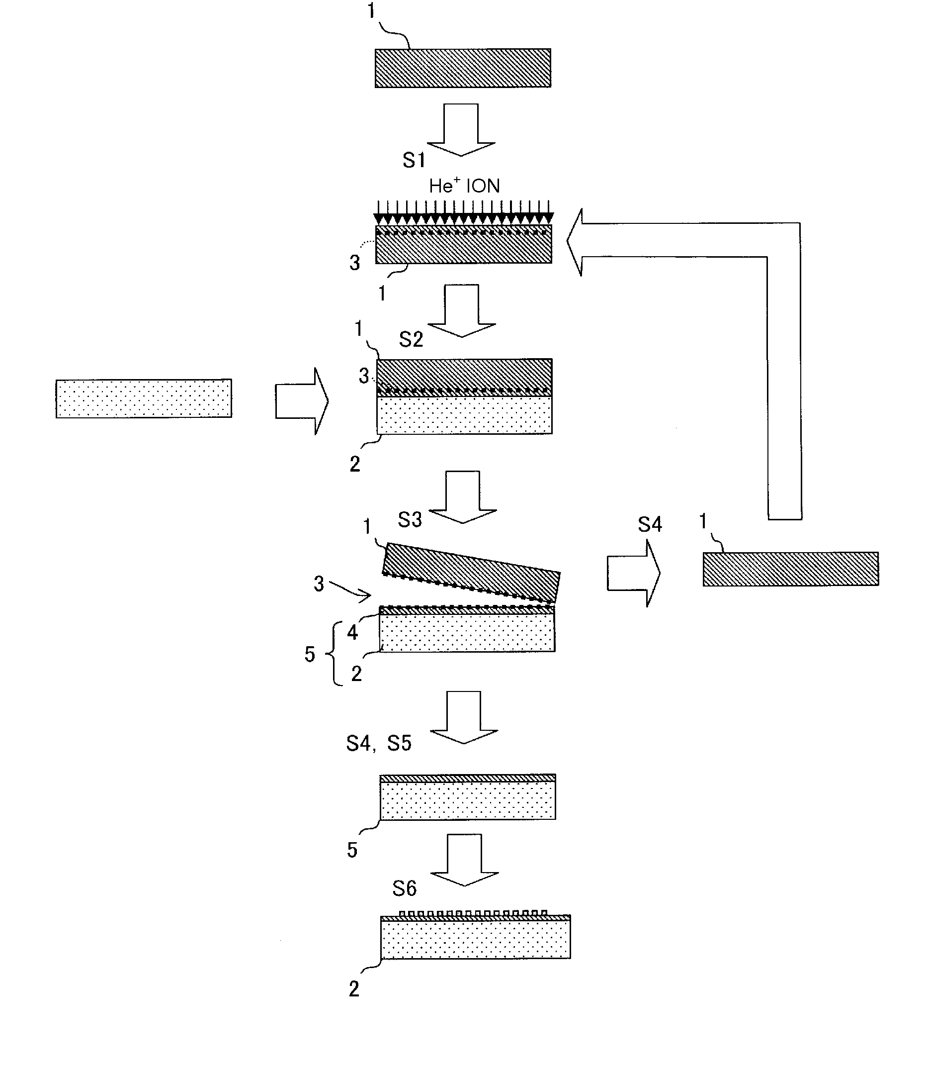
[0022]A method for producing a piezoelectric composite substrate according to a preferred embodiment of the present invention will be described below with reference to a method for producing a surface acoustic wave resonator as an example. In this preferred embodiment, LiNbO3 is preferably used as a piezoelectric material. A Si substrate is preferably used as a support substrate.

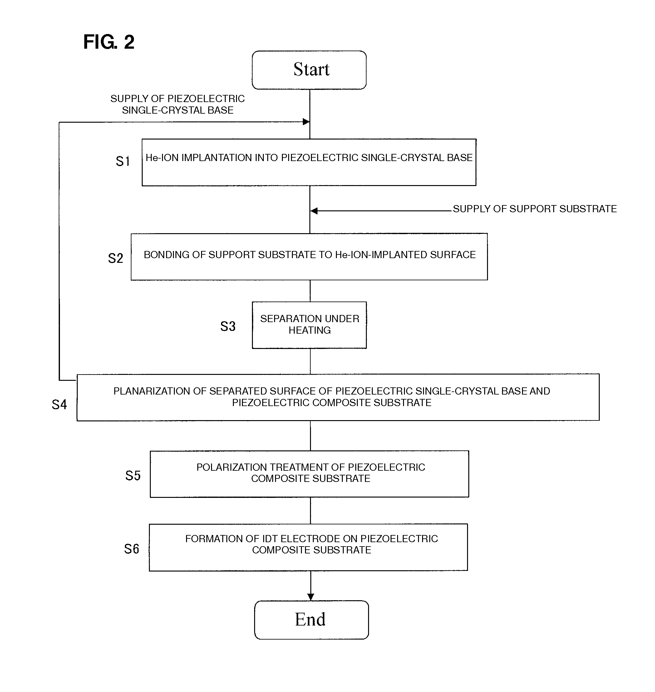
[0023]FIG. 2 shows a flow chart of the method for producing a surface acoustic wave resonator according to this preferred embodiment. FIG. 3 is a schematic view showing a piezoelectric composite substrate, a piezoelectric single-crystal base, and a support substrate in steps in the flow chart.

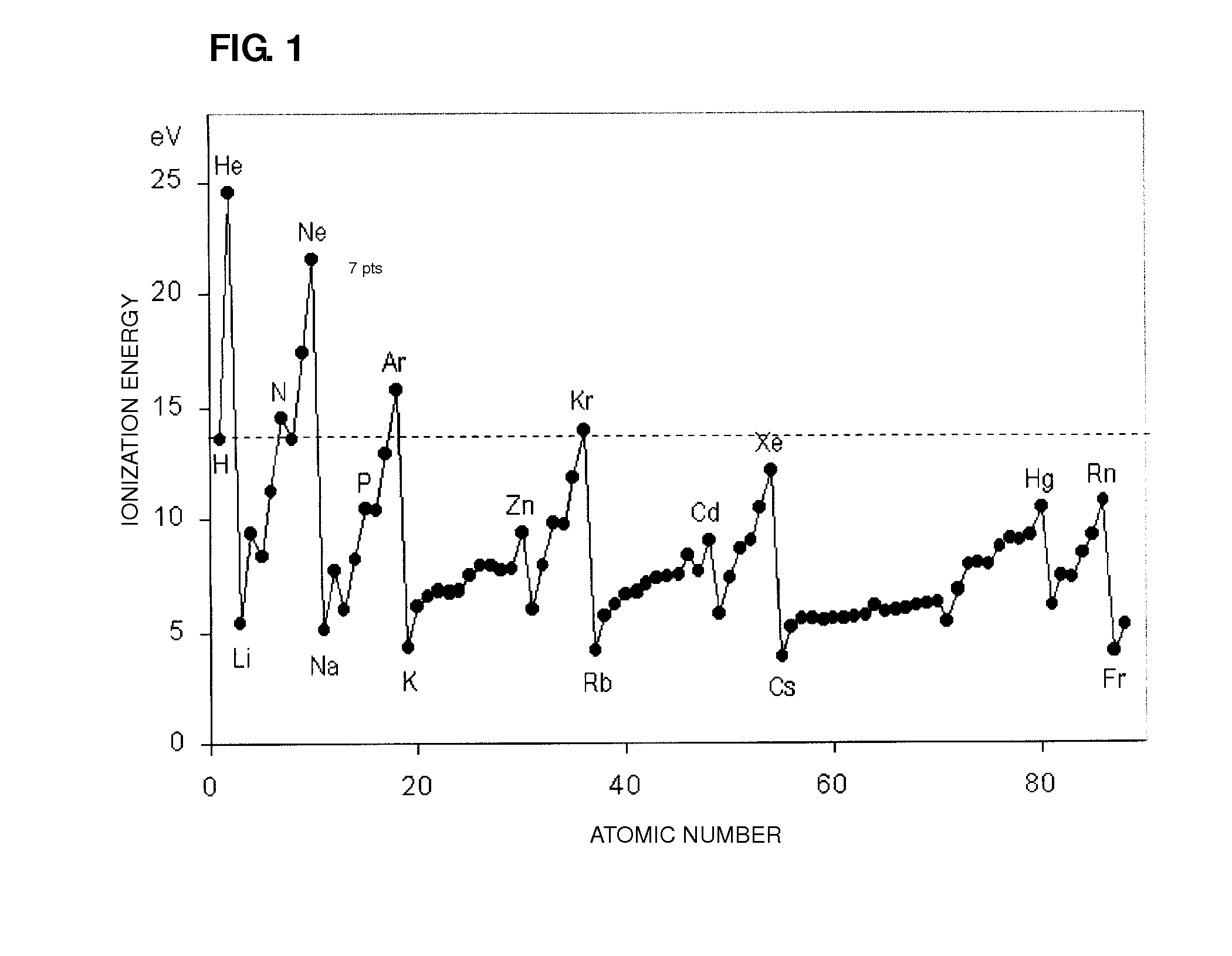
[0024]In this production process, an ion-implantation step (S1) of implanting He+ ions into a mirror-polished main surface of a piezoelectric single-crystal base 1 is performed. Here, the implantation energy of He+ ions is preferably set to about 150 KeV, for example. The dose level (density of implanted ions) is prefer...


PUM

PropertyMeasurementUnit
Densityaaaaaaaaaa
Energyaaaaaaaaaa
Piezoelectricityaaaaaaaaaa

Abstract

A method for producing a piezoelectric composite substrate having a single-crystal thin film of a piezoelectric material includes an ion-implantation step and a separation step. In the ion-implantation step, He+ ions are implanted into the single-crystal base made of the piezoelectric material to form localized microcavities in a separation layer located inside the single-crystal base and apart from a surface of the single-crystal base. In the separation step, the microcavities formed in the ion-implantation step are subjected to thermal stress to divide the separation layer of the piezoelectric single-crystal base, thereby detaching the single-crystal thin film.

Description

BACKGROUND OF THE INVENTION[0001]1. Field of the Invention[0002]The present invention relates to a method for producing a piezoelectric composite substrate having a single-crystal thin film made of a piezoelectric material.[0003]2. Description of the Related Art[0004]In recent years, piezoelectric elements including a piezoelectric composite substrate with a single-crystal thin film made of a piezoelectric material have been developed. The single-crystal thin film made of a piezoelectric material has been produced by a first production process including depositing a piezoelectric material, such as AlN or ZnO, using sputtering or CVD (for example, see Y. Osugi et al.; “Single Crystal FBAR With LiNbO3 and LiTaO3”, 2007 IEEE MTT-S International Microwave Symposium, pp. 873-876) or a second production process including polishing a single-crystal base made of a piezoelectric material (for example, see M. Bruel; “Silicon On Insulator Material Technology”, Electronics Letters, vol. 31, Iss...

Claims


Application Information

Patent Timeline
IPC IPC(8): B32B38/10C30B33/02H03H3/08H03H9/145
CPCH03H3/02H01L41/257H01L41/312H10N30/045H10N30/072
Inventor HAYAKAWA, NORIHIROIWAMOTO, TAKASHIKANDO, HAJIME
Owner MURATA MFG CO LTD
Why Eureka
Try Eureka