Method and system for multiplexer waveguide coupling

a technology of multiplexer and waveguide, applied in multiplex communication, optical elements, instruments, etc., can solve the problems of high coupling loss at the coupling interface, high packaging cost of the integrated optical circuit, and difficulty in fabricating these components using standard planar waveguide technology

Active Publication Date: 2010-05-13
INTERUNIVERSITAIR MICRO ELECTRONICS CENT (IMEC VZW) +2
View PDF6 Cites 56 Cited by
  • Summary
  • Abstract
  • Description
  • Claims
  • Application Information

AI Technical Summary

Benefits of technology

[0014]It is an object of the present invention to provide good methods and systems for all-optically multiplexing and / or demultiplexing radiation of substantially different wavelengths. It is an advantage of embodiments of the present invention that an integrated waveguide coupler and (de)multiplexer is provided based on a diffraction grating structure, the coupler being capable of coupling optical signals over a large wavelength span. The polarization of the light in the dielectric waveguides can be transverse electric, quasi transverse electric, transverse magnetic or quasi transverse magnetic. More specifically the integrated waveguide coupler according to embodiments of the present invention allows coupling of optical signals centered around two distinct wavelengths or wavelength bands, by exploiting the duplexer action of the diffraction grating structure. The grating structure may be a one-dimensional or a two-dimensional structure. In case of a two-dimensional grating structure, a system can be obtained wherein the performance is not sensitive to the polarization of the incident light, such that polarization independent integrated optical circuits may be obtained.
[0018]In the context of this invention, it is advantageous that the polarization of the light in the dielectric waveguides can be transverse electric, quasi transverse electric, transverse magnetic or quasi transverse magnetic. In photonic integrated circuits, the light used in the dielectric waveguides may be polarized (quasi) transverse electric (TE). Integrated lasers emit TE light. TE polarized light or quasi TE polarized light experiences lower losses in the dielectric waveguides, and the effective index contrast is larger for transverse electric (TE) polarized radiation than for transverse magnetic (TM), resulting in higher confinement (shorter bends, lower cross talk, etc.)
[0020]An optical device for all-optically multiplexing or demultiplexing light of substantially different predetermined wavelengths according to embodiments of the present invention comprises at least one first dielectric waveguide and at least one second dielectric waveguide formed on a substrate, the at least one first dielectric waveguide and the at least one second dielectric waveguide intersecting at an intersection, and a diffraction grating structure formed at the intersection. In embodiments according to the present invention, the diffraction grating structure is adapted for diffracting light of a first predetermined wavelength from the at least one first dielectric waveguide in a coupling direction, and for diffracting light of a second predetermined wavelength from the at least one second dielectric waveguide in substantially the same coupling direction, the first predetermined wavelength and the second predetermined wavelength being substantially different. The coupling direction thereby is substantially different from the normal direction on the average plane defined by the grating structure. The difference between the first predetermined wavelength and the second predetermined wavelength may for example be between 20 nm and 500 nm. The diffraction grating structure being adapted for diffracting light of a first predetermined wavelength from the at least one first dielectric waveguide in a coupling direction, and for diffracting light of a second predetermined wavelength from the at least one second dielectric waveguide in substantially the same coupling direction, may comprise the diffraction grating structure having at least one predetermined grating period, grating depth, grating layer thickness or grating duty cycle. The light in the at least one first dielectric waveguide and the light in the at least one second dielectric waveguide can be polarized (quasi) transverse electrically or (quasi) transverse magnetically. The incident light or outcoupling radiation can be polarized transverse electrically, transverse magnetically or both. This is advantageous in view of the applicability of the invention: the light of integrated lasers is mainly polarized (quasi) transversally electric. This light travels as TE polarized or quasi TE polarized light in the dielectric waveguides. Moreover, TE polarized light or quasi TE polarized light experiences lower scattering losses and a higher effective refractive index contrast allowing for example smaller bends and lower cross talk.

Problems solved by technology

Due to the large difference in mode size between the optical fiber and the integrated optical waveguide, this typically leads to high coupling losses at the coupling interface.
While these types of coupling interfaces provide lower coupling loss, the sub-micron alignment accuracy required to position the optical fiber with respect to the optical waveguide is very critical and implies therefore a high packaging cost of the integrated optical circuit.
Three dimensional spot-size converters allow low coupling losses between the integrated optical waveguide and a single mode optical fiber, but fabrication of these components using standard planar waveguide technology is difficult.
However, the use of this spot-size converter approach in high refractive index contrast devices always implies the need of a lensed optical fiber or high numerical aperture optical fiber, again resulting in the requirement of high alignment accuracy.
The optical bandwidth of this type of devices is however limited by the dispersive nature of the grating structure, implying that the angle, under which light is coupled out of the grating, when excited from the optical waveguide, changes as a function of wavelength.
Due to the limited numerical aperture of the optical fiber, wavelengths that deviate too much from the central wavelength, defined as the wavelength for which the angle of diffraction matches the tilt angle of the optical fiber, are less efficiently collected in the optical fiber.
As in typical applications this polarization is unknown and varying over time, the applicability of the one-dimensional grating structures is limited.
Besides the fact that fiber to chip coupling efficiencies comparable to the one-dimensional grating structure still have to be demonstrated, for some practical applications the optical bandwidth of the fiber-to-chip coupling efficiency is too small.
Whereas this is sufficient for applications requiring only a single optical wavelength or a set of closely spaced optical wavelengths, this is insufficient for other types of applications where the use of optical signals over a large wavelength span is required.
Due to the large wavelength span used in this application the use of a prior art waveguide grating coupler structure is no longer applicable, as its optical bandwidth is too small.

Method used


Image

  • Method and system for multiplexer waveguide coupling
  • Method and system for multiplexer waveguide coupling
  • Method and system for multiplexer waveguide coupling

Examples


first embodiment

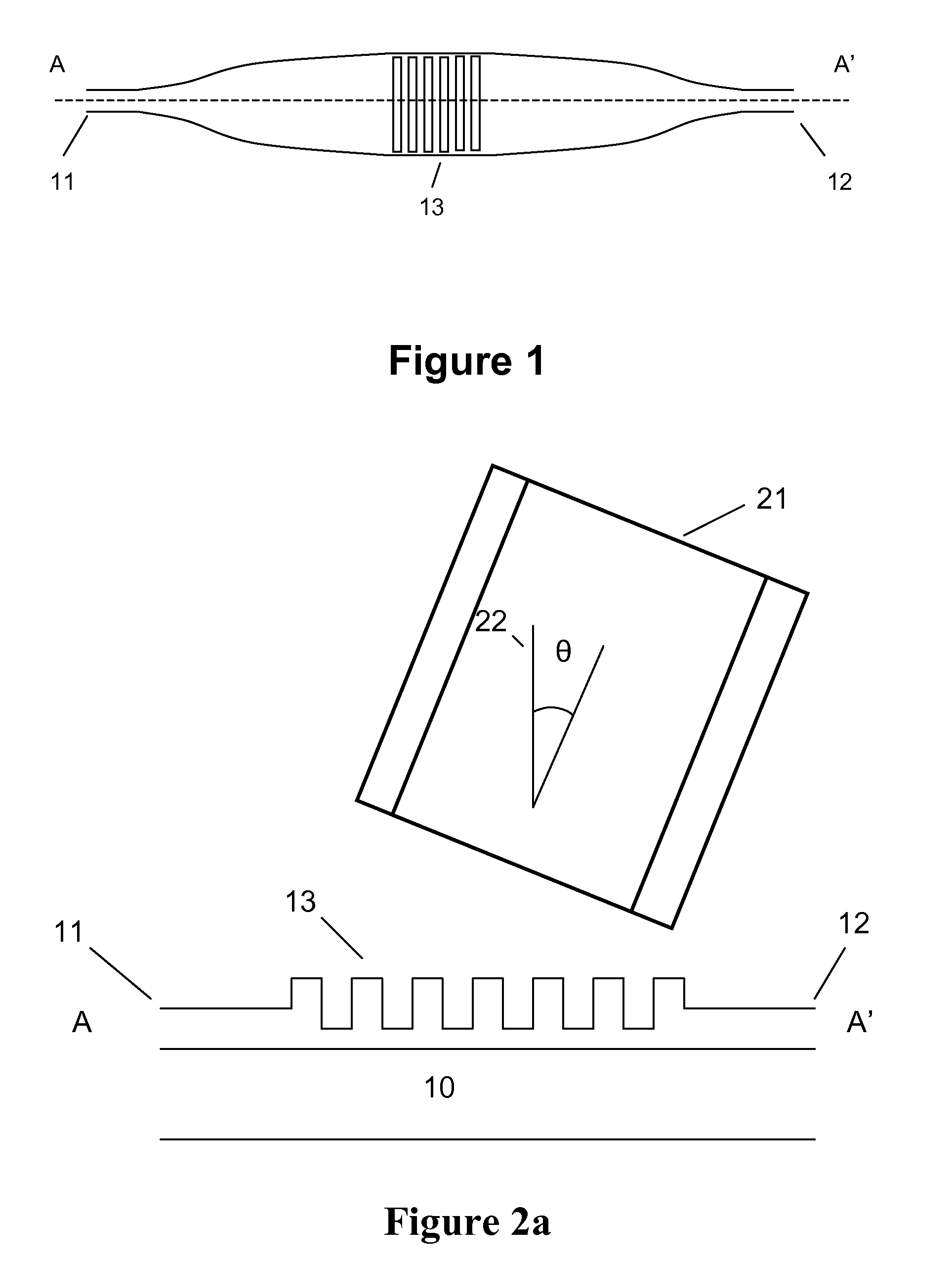
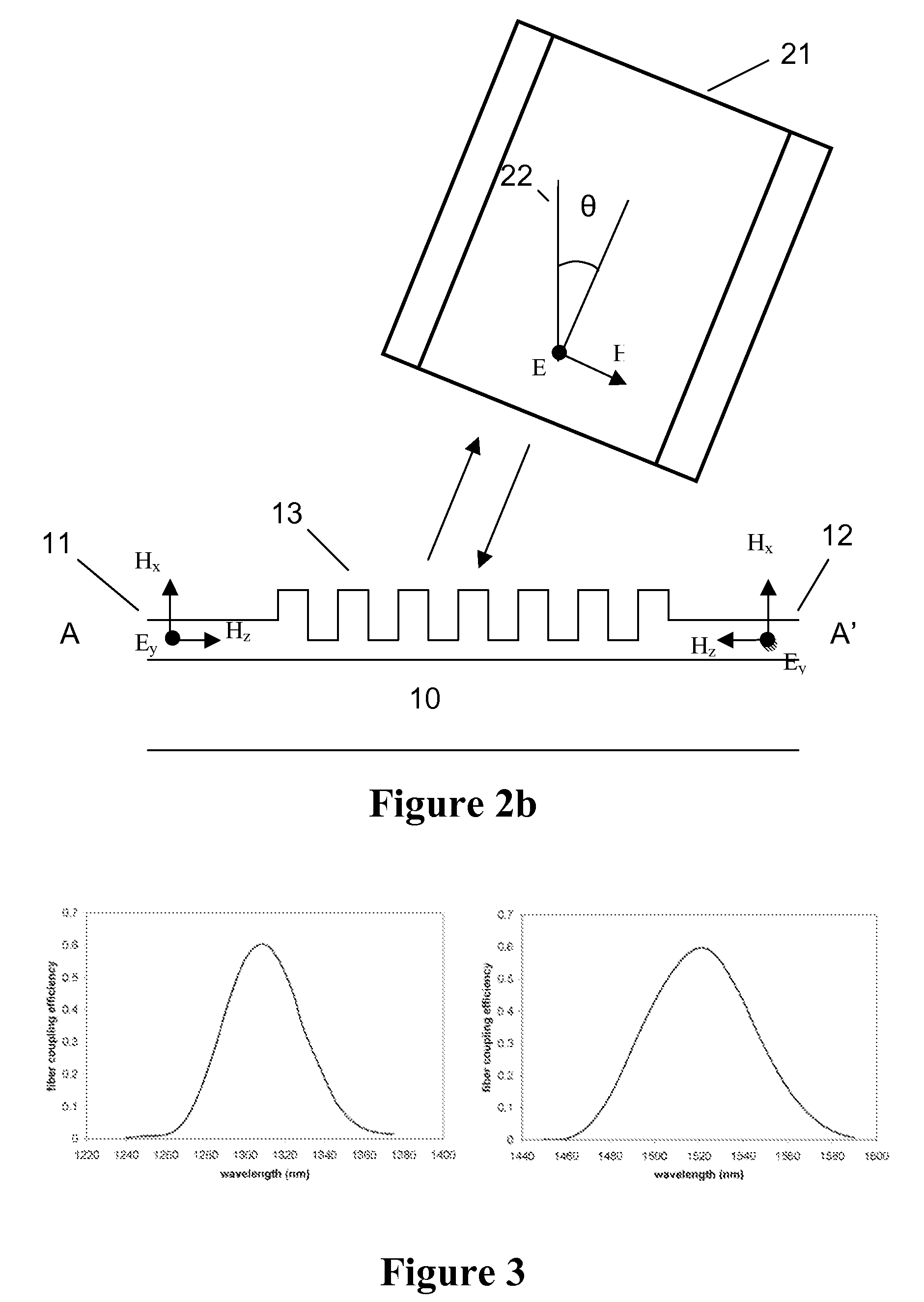
[0063]In a first embodiment, shown in FIGS. 1, 2a and 2b, the optical device in accordance with the present invention comprises a first dielectric waveguide 11 and a second dielectric waveguide 12 on a substrate 10, for example intersecting under a substantially straight angle, and a diffraction grating structure 13 at the intersection of both dielectric waveguides, such as for example a one-dimensional diffraction grating structure. Due to the dispersive properties of the grating structure, there exists a first wavelength or wavelength band for which radiation of that first wavelength traveling within the first dielectric waveguide 11 and exciting the grating structure is diffracted at an angle corresponding to an coupling direction and there exists a second wavelength or wavelength band, different from the first wavelength or wavelength band, for which radiation of that second wavelength traveling within the second dielectric waveguide 12 and exciting the grating structure is diff...

second embodiment

[0073]In a second embodiment according to the present invention, the polarization issue is tackled by using a two-dimensional diffraction grating structure as a coupler and multiplexer. FIG. 6 shows the layout of this embodiment, comprising 4 dielectric optical waveguides 41, 42, 43, 44 which intersect and which form a substantially right angle at the intersection. At the intersection of the 4 waveguides, a two-dimensional grating structure 45 is provided. The latter may be formed in any suitable way, for example by etching an array of holes or rods in the waveguide layer or in the waveguide cladding layer at the intersection or by defining e.g. a dielectric or metallic structured layer on top of the waveguide structure. Although FIG. 6 shows a periodic arrangement of holes, which define the two-dimensional grating structures, also non-periodic structures with composing elements other than holes may be used, i.e. the spacing, size and shape of the features composing the diffraction ...

third embodiment

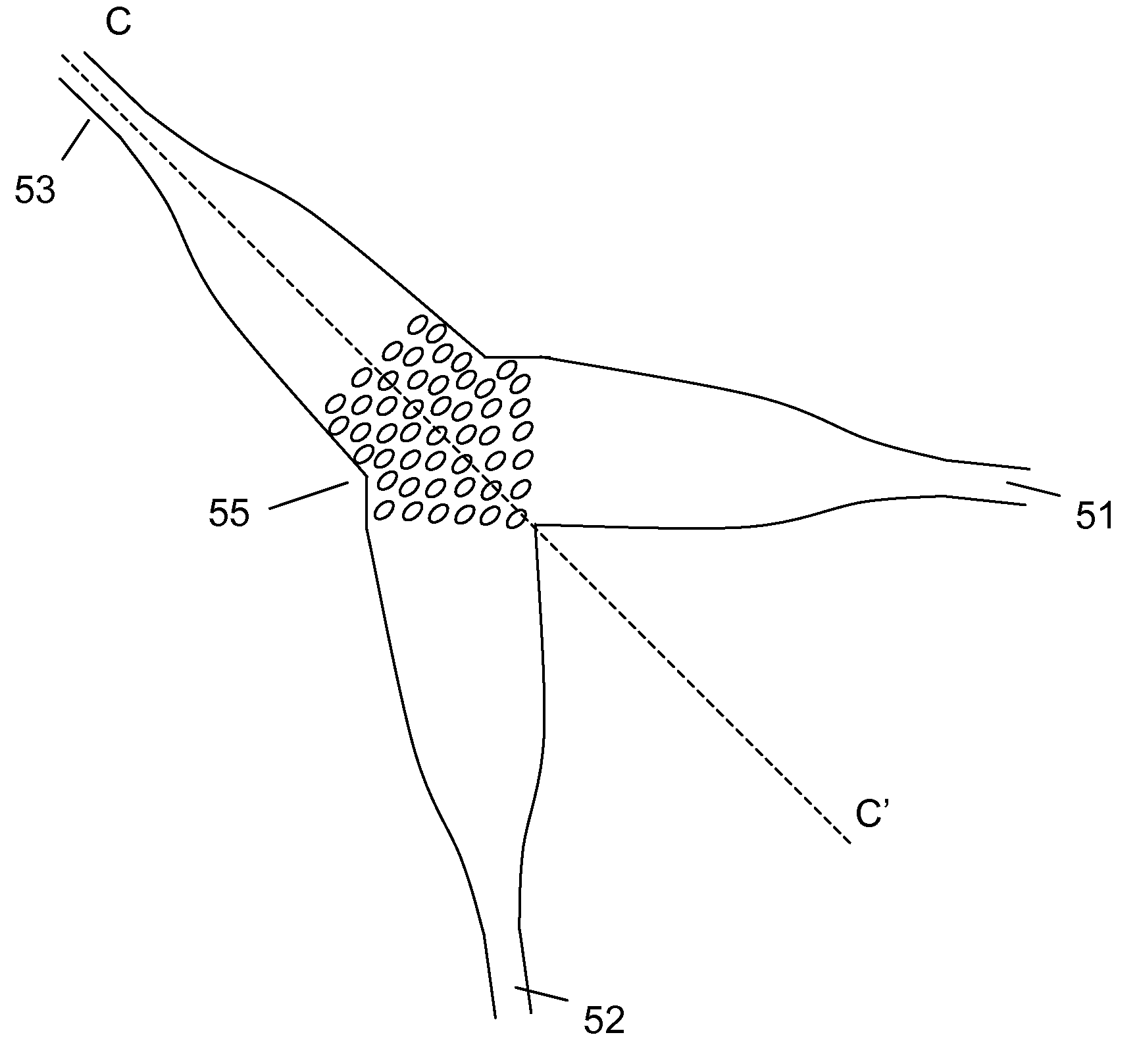
[0076]In a third embodiment according to the present invention, the polarization issue is tackled for a single wavelength or wavelength band by using a two-dimensional grating structure as a duplexer. An exemplary layout of this embodiment is shown in FIG. 7, comprising three optical dielectric waveguides 51, 52, 53, two of which (51, 52) form a substantially right angle, while the third dielectric waveguide 53 lies along the bisection line CC′ of the two former dielectric waveguides 51, 52. At the intersection of the dielectric waveguides, a two-dimensional grating structure 55 is formed, for example by etching an array of holes or rods in the waveguide layer or in the waveguide cladding layer or by defining e.g. a dielectric or metallic structured layer on top of the waveguide structure. Although FIG. 7 shows a periodic arrangement of holes, which define the two-dimensional grating structures, also non-periodic structures with composing elements other than holes may be used, i.e. ...


PUM


Abstract

An optical device for optically multiplexing or demultiplexing light of different predetermined wavelengths is provided, the optical device comprising at least one first waveguide (11) and at least one second waveguide (12) formed on a substrate (10), wherein the at least one first waveguide and the at least one second waveguide intersect at an intersection, comprising a diffraction grating structure (13) formed at the intersection. There exists a first wavelength or wavelength band travelling within the first waveguide (11) exciting the grating structure and being diffracted an angle corresponding to an outcoupling direction and there exists a second wavelength or wavelength band, different from the first wavelength or wavelength band, travelling within the second waveguide (12) exciting the grating structure and being diffracted at an angle corresponding to the same outcoupling direction. The two radiation beams comprising radiation of two different wavelengths or wavelength bands are spatially separated into the optical waveguides (11 and 12) or combined into single outcoupling direction, e.g. into a single optical element, e.g. a single optical fiber (21). An optical device may be used in local access communications such as fiber to the home, office or curb applications.

Description

FIELD OF THE INVENTION[0001]This invention relates to integrated optical components. More specifically it relates to integrated all-optical dielectric waveguide couplers and integrated wavelength multiplexer and demultiplexer circuits, methods and systems for designing such optical components and methods for coupling radiation between different radiation guides.BACKGROUND OF THE INVENTION[0002]Photonic integrated circuits hold the potential of creating low cost, compact optical functions. The application fields in which they can be applied are very diverse: telecommunication and data communication applications, sensing, signal processing, etc. These optical circuits comprise different optical elements such as light sources, optical modulators, spatial switches, optical filters, photodetectors, etc., the optical elements being interconnected by optical waveguides.[0003]Optical waveguides are typically implemented as solid dielectric light conductors, which allow to route light over t...

Claims


Application Information

Patent Timeline
Patent Type & Authority Applications(United States)
IPC IPC(8): H04J14/02G02B6/124G02B6/34
CPCG02B6/12007G02B6/126G02B6/4215G02B6/30G02B6/34G02B6/29317G02B6/4213
Inventor ROELKENS, GUNTHERVAN THOURHOUT, DRIESBAETS, ROELVAN DEN HOVEN, GERARD NICOLAAS
Owner INTERUNIVERSITAIR MICRO ELECTRONICS CENT (IMEC VZW)
Why Eureka
Try Eureka