Sic epitaxial substrate and method for producing the same

a technology of epitaxial substrate and substrate, which is applied in the direction of crystal growth process, polycrystalline material growth, crystal growth process, etc., can solve the problems of insufficiently preventing the occurrence of such defects as basal plane dislocations and screw dislocations, and the active layer of the active layer of the active layer of the conventional arts is problematically affected, so as to achieve the effect of improving the buffer layer

Inactive Publication Date: 2010-05-13
RES INST OF INNOVATIVE TECH FOR THE EARTH +1
View PDF9 Cites 42 Cited by
  • Summary
  • Abstract
  • Description
  • Claims
  • Application Information

AI Technical Summary

Benefits of technology

[0039]This arrangement uses a monocrystal SiC substrate having been subjected to a planarizing process. This improves the buffer layer and the active layer in uniformity of their film thicknesses and in flatness. This arrangement further reduces the number of crystal defects propagated from the monocrystal SiC substrate to the active layer and the number of new crystal defects occurring when the buffer

Problems solved by technology

While the techniques of Patent Literatures 2 to 4 do prevent occurrence of micropipe defects, they fail to sufficiently prevent occurrence of such defects as basal plane dislocations and screw dislocations.
Thus, such defects problematically occur in the active layer in these conventional arts.
However, for example, crystal defects other than micropipes, the crystal defects being inherent in the monocrystal SiC substrate, are likely to be propagated via the first epitaxial layer to the second epitaxial layer.
Thus, the technique problematically fails to prevent occurrence of crys

Method used


Image

  • Sic epitaxial substrate and method for producing the same
  • Sic epitaxial substrate and method for producing the same
  • Sic epitaxial substrate and method for producing the same

Examples


Embodiment Construction

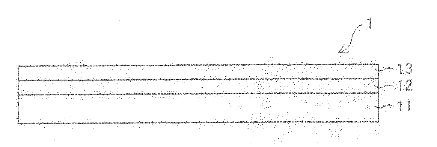
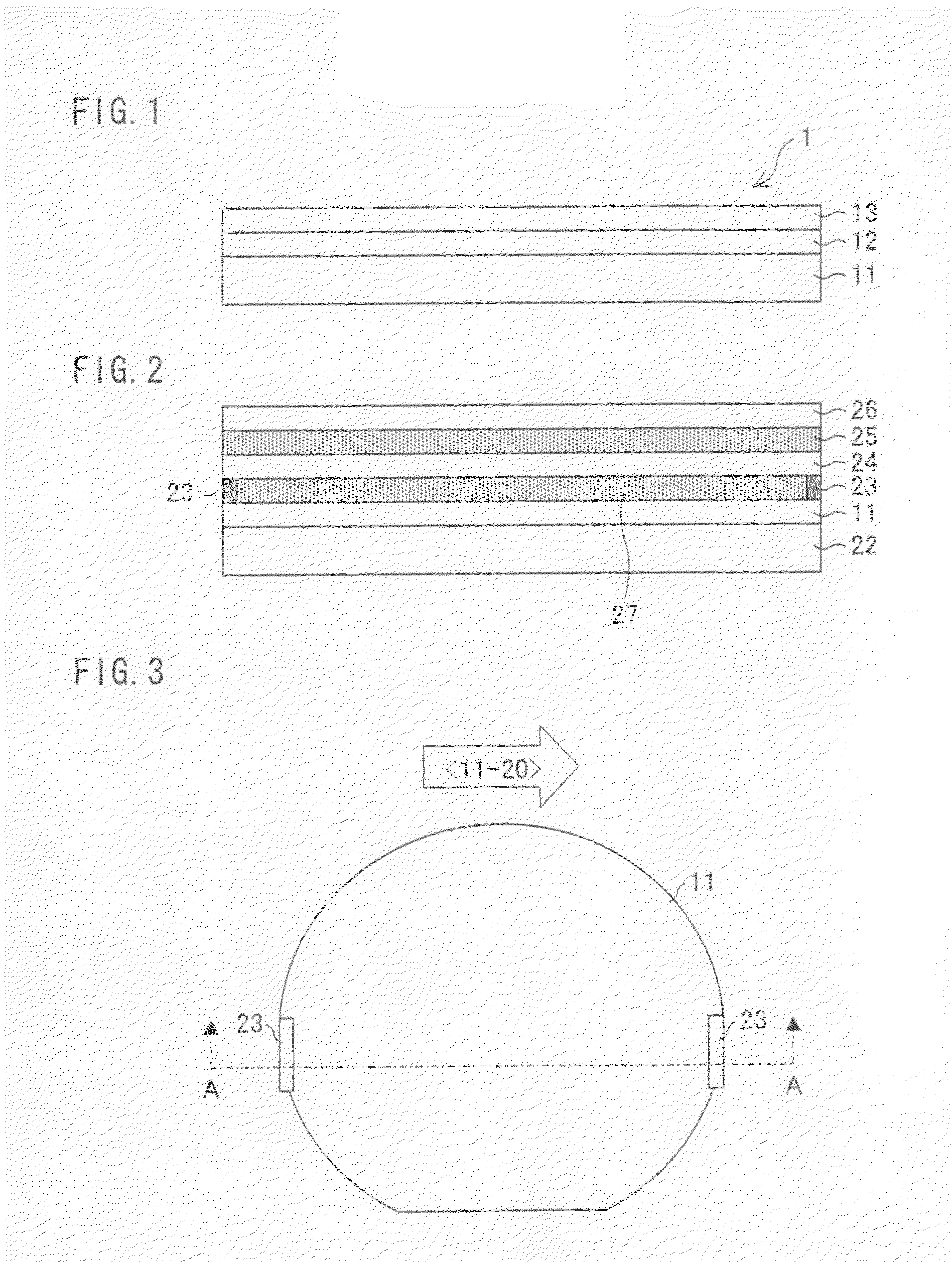
[0061]One embodiment of the present invention is described below. FIG. 1 is a cross-sectional view illustrating an arrangement of a monocrystal SiC epitaxial substrate 1 according to the present embodiment.

[0062]As illustrated in FIG. 1, the monocrystal SiC epitaxial substrate 1 includes a monocrystal SiC substrate 11; a buffer layer 12 formed on the monocrystal SiC substrate 11; and an active layer 13 formed on the buffer layer 12.

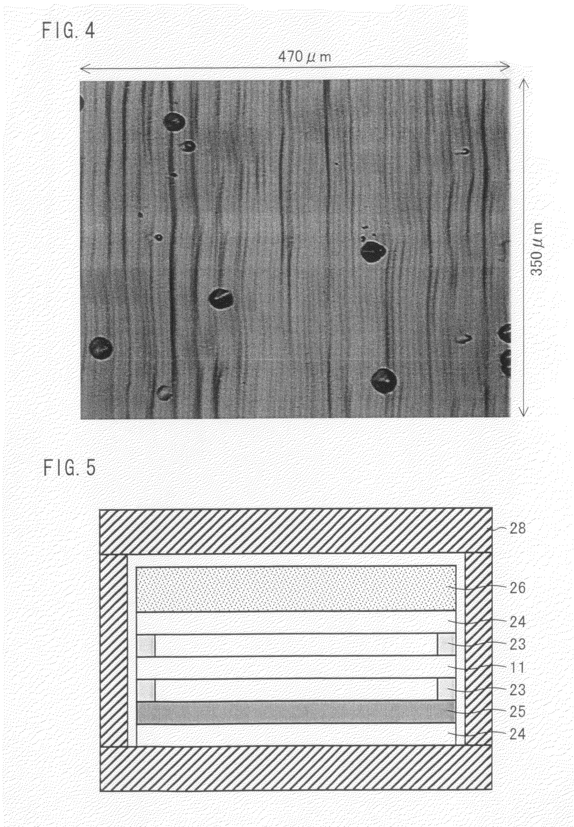
[0063]The monocrystal SiC substrate 11 may be conventionally known monocrystal SiC substrate (e.g., a commercially available monocrystal SiC substrate). The present embodiment used a 4H—SiC substrate having an 8-degree off angle along a direction indicated by . Further, the monocrystal SiC substrate 11 of the present embodiment had a surface on which the buffer layer 12 was formed, the surface having been planarized by chemical mechanical polishing (CMP) before the buffer layer 12 was formed. The planarization removed trace of polishing (polishing marks),...


PUM


Abstract

In one embodiment of the present invention, a monocrystal SiC epitaxial substrate is produced which includes a monocrystal SiC substrate; a buffer layer made of a first SiC epitaxial film formed on the monocrystal SiC substrate; and an active layer made of a second SiC epitaxial film formed on the buffer layer. The buffer layer is grown by heat-treating a set of the monocrystal SiC substrate, a carbon source plate, and a metal Si melt layer having a predetermined thickness and interposed between the monocrystal SiC substrate and the metal Si melt layer, so as to epitaxially grow monocrystal SiC on the monocrystal SiC substrate. The active layer is grown by epitaxially growing monocrystal SiC on the buffer layer by vapor phase growth method. This allows for production of a monocrystal SiC epitaxial substrate including a high-quality monocrystal SiC active layer being low in defects.

Description

TECHNICAL FIELD[0001]The present invention relates to a SiC epitaxial substrate including a SiC epitaxial film formed on a monocrystal SiC substrate, and also to a method for producing the SiC epitaxial substrate.BACKGROUND ART[0002]SiC (silicon carbide) is characterized as (i) excelling in heat resistance and mechanical strength, (ii) being resistant to radiation, (iii) being easily controllable for valence of electrons or holes by doping, and (iv) having a large forbidden band width. For reasons such as these, SiC is expected as a semiconductor material for next-generation power devices and high-frequency devices.[0003]Unfortunately, a monocrystal SiC substrate is inherently likely to have crystal defects caused by heat, such as a basal plane dislocation, a screw dislocation, and a micropipe. Further, a monocrystal SiC substrate likely has grain boundaries arising from nucleation.[0004]Thus, when an active layer made of monocrystal SiC is grown on a monocrystal SiC substrate by va...

Claims


Application Information

Patent Timeline
IPC IPC(8): B32B9/04C30B23/02H01L33/00
CPCC30B25/20C30B29/36H01L21/02378H01L21/02433H01L21/02447C30B29/06H01L21/02628H01L33/0054C30B13/00C30B25/02C30B25/18H01L21/02529
Inventor NAKAMURA, NOBUHIKOMATSUNAMI, TORUNISHIKAWA, KIMITO
Owner RES INST OF INNOVATIVE TECH FOR THE EARTH
Why Eureka
Try Eureka