
Atomic layer deposition process for manufacture of battery electrodes, capacitors, resistors, and catalyzers

a technology of atomic layer deposition and battery electrodes, which is applied in the direction of catalyst activation/preparation, metal/metal-oxide/metal-hydroxide catalysts, fixed capacitors, etc., can solve the problems of dielectric films that are difficult to manufacture on pcbs, limited equipment capabilities, and size limitations, and achieve low serial resistance, no leakage, and no damage to the surrounding electronics

Inactive Publication Date: 2010-05-20
LAOR CONSULTING +1
View PDF78 Cites 32 Cited by
  • Summary
  • Abstract
  • Description
  • Claims
  • Application Information

AI Technical Summary

Benefits of technology

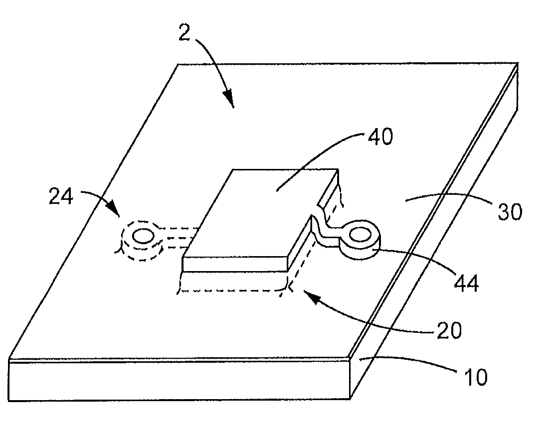
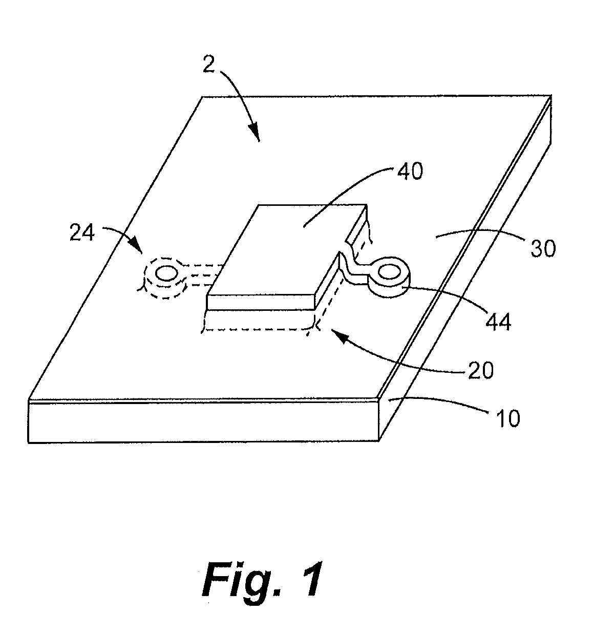
[0007]ALD manufacturing technology is developed to a high level, with deposition equipment available from several companies. See, e.g. http: / / en.wikipedia.org / wiki / Atomic_layer_deposition, www.beneq.com, www.oxford-instruments.com, www.cambridgenanotech.com, www.sundewtech.com, which are incorporated by reference in their entirety. Observing ALD-manufactured capacitors on Silicon substrates further demonstrates the benefits over other known manufacturing methods. For example, deposited Al2O3 forms a high quality layer of amorphous material on almost any material. More particularly, ALD dielectric films are exceptionally defect free, stress free and pinhole free down to the 1-2 monolayers thickness (0.6-0.8 nm). This unmatched characteristic is due to the unique, layer-by-layer growth mechanism of ALD films. Metal pads that are commonly utilized in the PCB manufacturing technology are (comparatively) highly irregular, porous and defected on a microscopic scale. Using ALD technology overcomes such deficiencies in part by the ability to conform to difficult topologies (of the underlying material). This is in contrast to sputtered or CVD dielectric films that have particular difficulties at creating uniform low thicknesses.
[0008]The tolerance in capacitance of the ALD deposited capacitor will depend in part on the tolerance of the metal patterning. This is due to the high accuracy in thickness of the ALD dielectric layer. Thickness variations are below 1% standard deviation and under 4% peak-to-peak. Thus, uniformity of thickness of the ALD layered material and improved surface consistency also leads to improved performance of the microelectronic component.
[0009]In addition to deposition on PCB materials, ALD technology may also be used for deposition of capacitors on chip carriers. This will enable construction of high capacitance, low inductance and low resistance bypass capacitors very near to the chip itself. The bypassing performance will substantially improve in part due to the short distance between the chip and the capacitor, and in part due to the lower inductance of the capacitor itself.
[0016]According to yet another embodiment, a method of manufacturing sintered capacitors using ALD is disclosed. These sintered capacitors will have fully monolithic structure, no leakage, no heat loss, low serial resistance and inductance, long life at elevated temperatures, induce no damage to the surrounding electronics upon failure and will be capable of full AC operation. The sintered capacitors manufactured according to this embodiment have a specific capacity, by way of example but not limitation, of 25 VμF / mm3-3.5 times higher then Tantalum capacitors, and 35 times higher then Aluminum capacitors. The sintered capacitors manufactured by this method are also disclosed in one embodiment of the present disclosure.
[0017]According to yet another embodiment, a catalyzer and method of manufacturing a catalyzer constructed of a porous material with the catalyst material deposited on the surface of the porous material by ALD technology is disclosed. The ALD process minimizes catalyst thickness while penetrating deep into the pores to achieve high surface area in the catalyzer.
[0021]a second electrode formed in the remaining volume to complement to the first electrode and the dielectric layer and substantially completing the 100% fill ratio.

Problems solved by technology

The size limitation is due to the limited capabilities of the equipment used for PCB assembly, namely pick-and-place tools.
However, dielectric films have been difficult to manufacture on PCBs due to the temperature limitation of about 250° C. of FR4 and Polyimid.
However, none of these technologies has been perfected in the PCB manufacturing field.
Metal pads that are commonly utilized in the PCB manufacturing technology are (comparatively) highly irregular, porous and defected on a microscopic scale.
This is in contrast to sputtered or CVD dielectric films that have particular difficulties at creating uniform low thicknesses.

Method used


Image

  • Atomic layer deposition process for manufacture of battery electrodes, capacitors, resistors, and catalyzers
  • Atomic layer deposition process for manufacture of battery electrodes, capacitors, resistors, and catalyzers
  • Atomic layer deposition process for manufacture of battery electrodes, capacitors, resistors, and catalyzers

Examples


Embodiment Construction

[0043]As discussed above, ALD is a manufacturing technique that allows one or more layers of atomic-scale precursor materials to be deposed on a surface, and has several benefits over other methods of manufacturing, including but not limited to operating at low pressures and temperatures, providing consistent and reliable atomic structures, and achieving uniform coating thickness at exposed and hidden surfaces that are not achievable with previous technologies. (See Appendix A to the U.S. Provisional Patent Application Nos. 61 / 028,383 and 61 / 028,402 for additional information on ALD technologies.) A typical ALD process may be summarized as comprising multiple cycles, with each cycle comprising two precursor stages (where two precursor materials are introduced) and two purge stages.

[0044]In the first precursor stage, the selected first precursor is introduced in to a reaction chamber for the purpose of reacting with a material. For example, Trimethyl Aluminum (TMA) may be used as a p...


PUM

PropertyMeasurementUnit
Fractionaaaaaaaaaa
Timeaaaaaaaaaa
Temperatureaaaaaaaaaa

Abstract

The present disclosure relates generally to the field of sequential surface chemistry. More specifically, it relates to products and methods for manufacturing products using Atomic Layer Deposition (“ALD”) to depose one or more materials onto a surface. ALD is an emerging variant of Chemical Vapor Deposition (“CVD”) technology with capability for high-quality film deposition at low pressures and temperatures, which may produce defect-free films, on a macroscopic scale, at any given thickness. The present disclosure includes, in varying embodiments, methods of manufacturing microelectronic assemblies and components such as battery electrodes, capacitors, resistors, catalyzers and PCB assemblies by ALD, and the products manufactured by those methods.

Description

CROSS REFERENCE TO RELATED APPLICATIONS[0001]The present application claims the benefit of U.S. Provisional Patent Application Nos. 61 / 028,383 and 61 / 028,402, both filed Feb. 13, 2008, the entire contents of which are incorporated herein by reference.BACKGROUND OF THE INVENTION[0002]The present invention relates generally to the field of sequential surface chemistry. More specifically, it relates to products and methods for manufacturing products using Atomic Layer Deposition (“ALD”) to depose one or more materials onto a surface. ALD is considered by some to be a variant of Chemical Vapor Deposition (“CVD”) technology, but with improved capability for high-quality, atomic-scale film depositions at low temperatures. The ALD technology was developed in part for the purposes of targeting deposition of materials for Silicon integrated circuit (“IC”) production. ALD is a relatively new method of Silicon IC manufacturing. ALD technology is highly efficient and may be enabled for use in a...

Claims


Application Information

Patent Timeline
IPC IPC(8): H01G4/005H01M4/00B05D5/12B01J35/10
CPCB01J23/40Y10T29/49002H01G4/33H01G9/0032H01G9/07H01G9/15H01M4/0428H01M4/64H05K1/092H05K1/162H05K2201/0116H05K2201/0179H05K2201/09763H05K2203/1131B01J37/0238Y02E60/10Y02E60/13
Inventor LAOR, HERZEL
Owner LAOR CONSULTING
Learn More