Very high speed FRAM for replacing SRAM

a framing and sram technology, applied in the field of ferroelectric random access memory, can solve the problems of slow access time, slow speed of one transistor-one capacitor framing, and time-consuming for driving the plate line, so as to reduce the parasitic capacitance of the local bit line, enhance the framing performance, and high speed framing

Inactive Publication Date: 2010-06-03
KIM JUHAN
View PDF15 Cites 12 Cited by
  • Summary
  • Abstract
  • Description
  • Claims
  • Application Information

AI Technical Summary

Benefits of technology

[0010]In the present invention, new memory architecture is realized for replacing SRAM with very high speed FRAM. In order to enhance performance of the FRAM, short bit line architecture is applied, such that bit lines are multi-divided into short lines for reducing parasitic capacitance of the local bit line. With lightly loaded local bit line, the local bit line is quickly charged and discharged for reading and writing. Furthermore, ferroelectric capacitor of the FRAM is proportionally reduced with lightly loaded local bit line, which reduces memory cell size as well.
[0011]In order to realize high speed operation, the FRAM cell stores a non-inverting data and an inverting data, which need not a reference voltage when sensing the memory cell, wherein the FRAM cell comprises four transistors and two capacitors. More specifically, the memory cell is composed of a first ferroelectric capacitor for storing a non-inverting data, a second ferroelectric capacitor for storing an inverting data, a first access transistor connecting to the first ferroelectric capacitor, a second access transistor connecting to the second ferroelectric capacitor, a first reset transistor connecting to the first ferroelectric capacitor, and a second reset transistor connecting to the second ferroelectric capacitor. With the reset transistors, unselected memory cells are not disturbed even though bit lines are swung from high to low or low to high during read and write operation, because the reset transistors strongly force a middle voltage to storage nodes of the ferroelectric capacitor while a plate line of the ferroelectric capacitors are forced to the middle voltage, which avoids undesirable polarization to the unselected memory cells. In the present invention, the performance is improved for replacing the SRAM, and the ferroelectric capacitor is reduced with the short bit line memory architecture for reducing chip area, even though the ferroelectric material is added for fabricating the chip. In general, two more masks are required to add the ferroelectric capacitor to the CMOS process.
[0012]Furthermore, the stored data in the memory cell is not erased after power is off, so that the non-volatile cache memory including the FRAM is very useful for various applications. For example, cache memory data are still remained after power is off, so that very quick booting is possible in computer, while most of computer is very slowly booted when power is on in these days. Another application is in mobile computing, such that a mobile processor can be turn off when no input is asserted, and then quickly booted when an input is asserted because the non-volatile cache memory stores cache data. Thus, long battery life is realized. In addition, power consumption is significantly reduced because charging and discharging current of the capacitor and the local bit line is reduced when operating.

Problems solved by technology

And access time is slow because there is a waiting time before the bit line is redistributed by the charges of the ferroelectric capacitor.
And a problem with the conventional one transistor-one capacitor FRAM is slow speed, because the plate line of the capacitor is driven by a plate line driver circuit from ground voltage to high voltage for reading and writing.
Driving the plate line takes time and adding the driver circuit occupies more chip area.
Even though those hierarchical bit line architectures have been applied for improving the FRAM, the FRAM with the prior arts is not fast than SRAM, not denser than DRAM and not denser than flash memory.

Method used


Image

  • Very high speed FRAM for replacing SRAM
  • Very high speed FRAM for replacing SRAM
  • Very high speed FRAM for replacing SRAM

Examples


Embodiment Construction

)

[0027]Reference is made in detail to the preferred embodiments of the invention. While the invention is described in conjunction with the preferred embodiments, the invention is not intended to be limited by these preferred embodiments. On the contrary, the invention is intended to cover alternatives, modifications and equivalents, which may be included within the spirit and scope of the invention as defined by the appended claims. Furthermore, in the following detailed description of the invention, numerous specific details are set forth in order to provide a thorough understanding of the invention. However, as is obvious to one ordinarily skilled in the art, the invention may be practiced without these specific details. In other instances, well-known methods, procedures, components, and circuits have not been described in detail so that aspects of the invention will not be obscured.

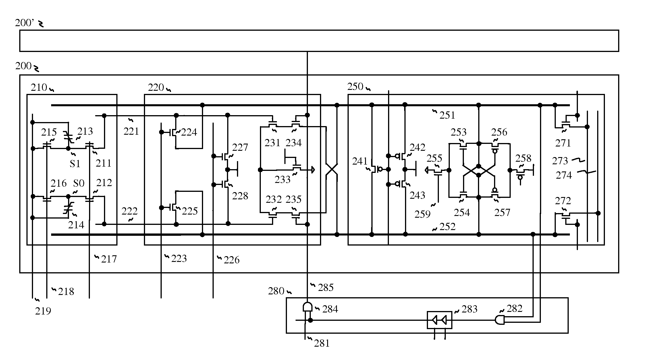
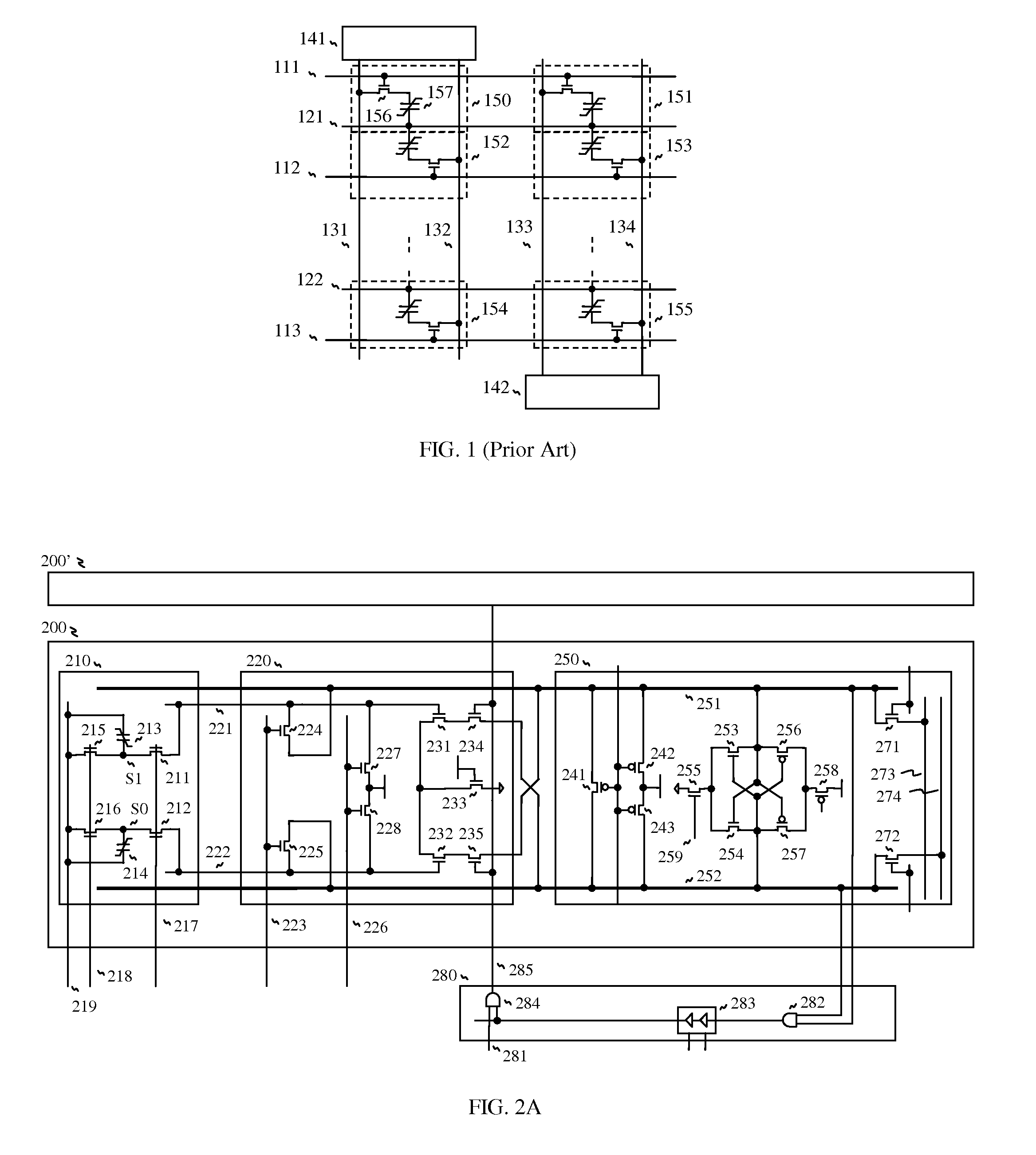
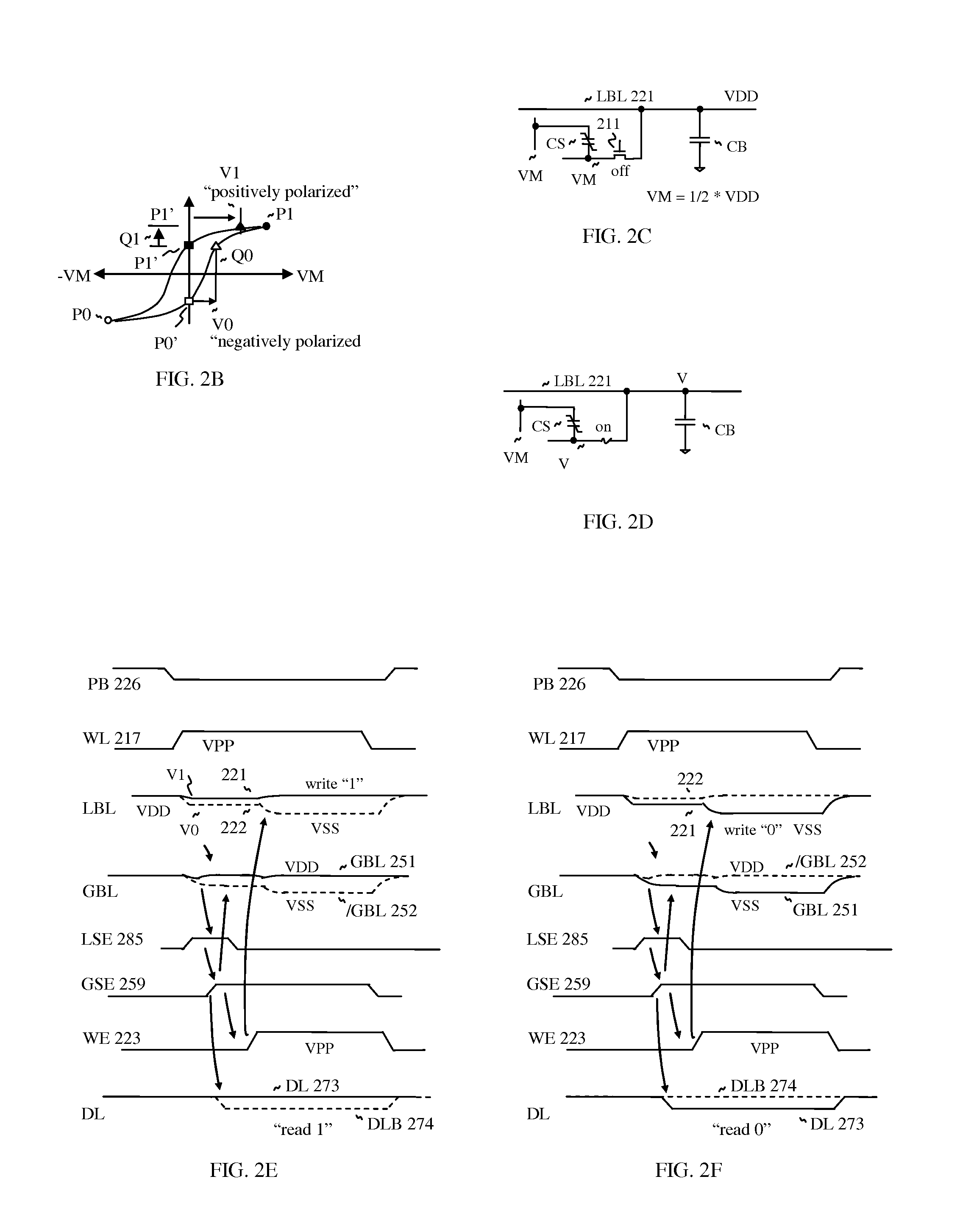
[0028]In the present invention, very high speed FRAM for replacing SRAM is realized as shown FIG. 2...


PUM


Abstract

For replacing SRAM with very high speed FRAM, new memory architecture is realized such that plurality of FRAM cells is connected to a local bit line pair, a local sense amp is connected to the local bit line pair, a global sense amp is connected to the local sense amp through a global bit line pair, and a locking signal generator is connected to the global sense amp for generating a locking signal which disables the local sense amp after reading for quick write-back operation. With short bit line architecture, bit lines are multi-divided for reducing parasitic capacitance of the local bit line, which realizes to reduce the ferroelectric capacitor proportionally. The FRAM cell includes an access transistor pair, a ferroelectric capacitor pair for storing positive data and negative data, and a reset transistor pair for resetting storage nodes. And various circuits for implementing the memory are described.

Description

CROSS REFERENCE TO RELATED APPLICATION[0001]The present invention is a continuation of application Ser. No. 12 / 253,997, filed on Oct. 19 2008, and application Ser. No. 12 / 471,472, filed on May 26 2009, which are herein incorporated by reference.FIELD OF THE INVENTION[0002]The present invention relates generally to integrated circuits, in particular to FRAM (Ferroelectric Random Access Memory).BACKGROUND OF THE INVENTION[0003]FRAM (Ferroelectric Random Access Memory) is a type of non-volatile memory device that uses such a ferroelectric capacitor and preserves stored information even when the power is off. Additionally, the FRAM has high-speed access, less power consumption, and excellent shock-resistance. Accordingly, the FRAM would be expected to be used as a main storage device for various electronic devices and equipment, such as computers, networks and mobile devices.[0004]In the FRAM, a memory cell is composed of the ferroelectric capacitor and a pass transistor, and which stor...

Claims


Application Information

Patent Timeline
Patent Type & Authority Applications(United States)
IPC IPC(8): G11C11/22G11C11/24G11C7/00G11C7/02
CPCG11C11/22G11C7/18
Inventor KIM, JUHAN
Owner KIM JUHAN
Why Eureka
Try Eureka