Acoustic resonator and its fabricating method

a technology of acoustic resonators and fabrication methods, applied in the direction of device details, device material selection, device details, etc., can solve the problem of inability to realize high electromechanical coupling coefficient, and achieve the effect of high q value, and increasing electromechanical coupling coefficien

Inactive Publication Date: 2010-06-17
SONY CORP
View PDF8 Cites 61 Cited by
  • Summary
  • Abstract
  • Description
  • Claims
  • Application Information

AI Technical Summary

Benefits of technology

[0020]In the acoustic-resonator fabricating method of the present invention, a step of forming the piezoelectric layer includes a step of forming a tensile stress layer in which tensile stress is present and a step of forming a compression stress layer in which compression stress is present, and the tensile stress layer and the compression stress layer are formed so that the tensile stress in the tensile stress layer and the compression stress in the compression stress layer cancel each other. The occurrence of a large bent of a piezoelectric layer in which only tensile stress or compression stress is present is prevented, and the electromechanical coupling coefficient is increased.
[0021]In the acoustic resonator of the present invention, the piezoelectric layer includes a tensile compression layer in which tensile stress is present and a compression stress layer in which compression stress is present, and the tensile stress in the tensile stress layer and the compression stress in the compression stress layer are adjusted to cancel each other. The occurrence of a large bent of a piezoelectric layer in which only tensile stress or c

Problems solved by technology

A problem to be solved is the point that, in an acoustic resonator with an air-bridge structure, a high el

Method used


Image

  • Acoustic resonator and its fabricating method
  • Acoustic resonator and its fabricating method
  • Acoustic resonator and its fabricating method

Examples


first embodiment

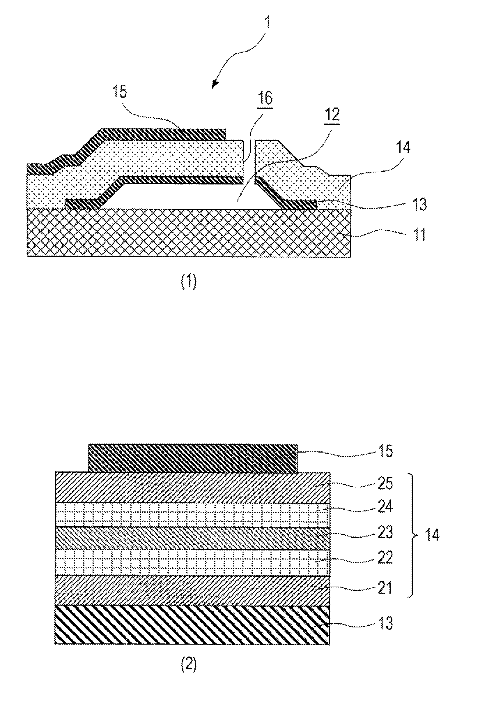
[0032]an embodiment according to an acoustic resonator of the present invention will be described using FIG. 1. Part (1) of FIG. 1 is a sectional view schematically illustrating the structure of the acoustic resonator, and part (2) of FIG. 1 illustrates an enlarged sectional view of a piezoelectric layer.

[0033]As shown in FIG. 1, a first electrode (lower electrode) 13 is formed on the top face of a supporting substrate 11 so as to cover an air layer 12. That is, the air layer 12 is enclosed by the first electrode 13. The first electrode 13 is made of, for example, molybdenum (Mo) and is formed to have a thickness of, for example, 230 nm. The first electrode 13 may be formed using, besides molybdenum, a metal material such as tungsten, tantalum, titanium, platinum, ruthenium, gold, aluminum, copper, or the like. The first electrode 13 may alternatively be formed of a plurality of layers made of the electrode material.

[0034]A piezoelectric layer 14 is formed on the first electrode 13....

second embodiment

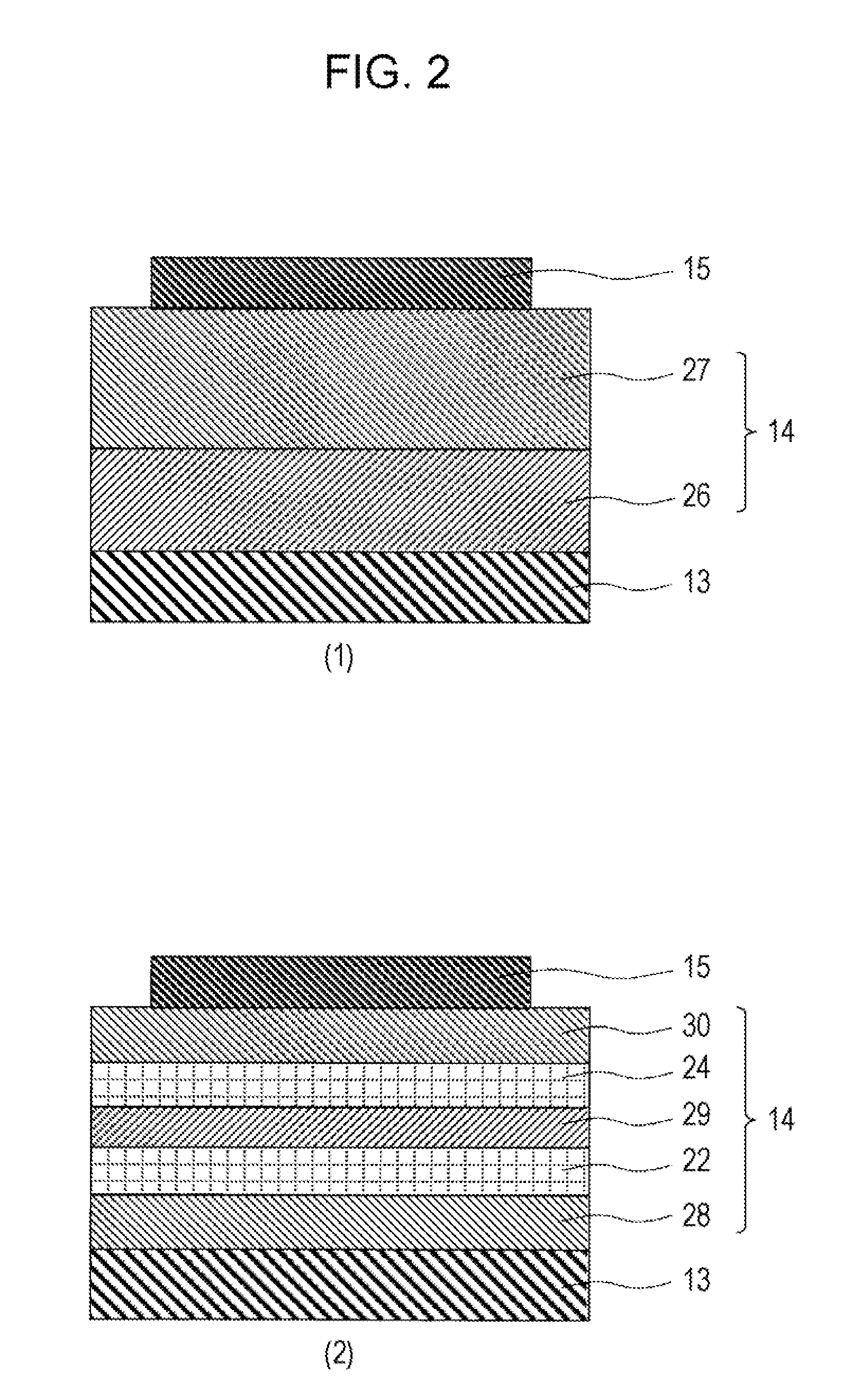
[0044]As shown in part (1) of FIG. 2, an acoustic resonator of the second embodiment has a structure similar to the foregoing acoustic resonator 1 except for the structure of the piezoelectric layer 14. Thus, the structure of the piezoelectric layer 14 will herein be described. The piezoelectric layer 14 is formed by staking, on the first electrode 13 formed on the supporting substrate 11 so as to cover the air layer 12, which has been described using FIG. 1, a compression stress layer 26 having compression stress and a tensile stress layer 27 having tensile stress, which is formed on the compression stress layer 26. Furthermore, the upper electrode 15 is formed on the tensile stress layer 27.

[0045]The thickness of the layers is, for example, as follows. The compression stress layer 26 has a thickness of 500 nm. The tensile stress layer 27 has a thickness of 500 nm. Thus, the thickness of the entire piezoelectric layer 14 is 1 μm.

[0046]In addition, the piezoelectric layer 14 is in a...

third embodiment

[0048]As shown in part (2) of FIG. 2, an acoustic resonator of the third embodiment has a structure similar to the foregoing acoustic resonator 1 except for the structure of the piezoelectric layer 14. Thus, the structure of the piezoelectric layer 14 will herein be described. The piezoelectric layer 14 is formed by sequentially staking, on the first electrode 13 formed on the supporting substrate 11 so as to cover the air layer 12, which has been described using FIG. 1, a tensile stress layer 28, the buffer layer 22, a compression stress layer 29, the buffer layer 24, and a tensile stress layer 30. The buffer layer 22 is provided between the tensile stress layer 28 and the compression stress layer 29 and is formed to alleviate tensile stress in the tensile stress layer 28 and compression stress in the compression stress layer 29. The buffer layer 22 is formed using, for example, an aluminum nitride layer having 0 stress or, for example, tensile stress or compression stress of 100 M...


PUM


Abstract

A piezoelectric layer has a multilayer structure including a tensile stress layer and a compression stress layer. The mechanical strength of the piezoelectric layer is increased to prevent the occurrence of cracks and to realize a high electromechanical coupling coefficient. An acoustic resonator 1 includes a first electrode 13 including at least one conductive layer, a piezoelectric layer 14 including a plurality of layers, the piezoelectric layer 14 being formed adjacent to the top face of the first electrode 13, and a second electrode 15 including at least one conductive layer, the second electrode 15 being formed adjacent to the top face of the piezoelectric layer 14. The piezoelectric layer 14 includes a tensile compression layer 23 in which tensile stress is present and compression stress layers 21 and 25 in which compression stress is present. The tensile stress in the tensile stress layer 23 and the compression stress in the compression stress layers 22 and 25 are adjusted to cancel each other.

Description

TECHNICAL FIELD[0001]The present invention relates to an acoustic resonator and its fabricating method for preventing damage to a piezoelectric layer.BACKGROUND ART[0002]In recent years, as cellular phones and personal mobile information terminals (PDA: Personal Digital Assistance) have become more sophisticated and faster, there has been an increasing demand to reduce the size and cost of high-frequency filters which are contained in these communication devices and which operate in a range from a few hundred MHz to a few GHz. A potential candidate for a high-frequency filter satisfying the demand is a filter using a thin film bulk acoustic resonator (abbreviated as FBAR hereinafter), which can be formed using semiconductor manufacturing techniques.[0003]As a representative example of FBAR, there is a structure called an air bridge type (e.g., see K. M. Lakin, “Thin Film Resonators and Filters”, Proceedings of the 1999 IEEE Ultrasonics Symposium, Vol. 2, p. 895-906, October 1999 (he...

Claims


Application Information

Patent Timeline
IPC IPC(8): H01L41/04B05D5/12H01L41/09H01L41/18H01L41/22H01L41/316H03H3/02H03H9/17
CPCH03H3/02H03H9/02015H03H2003/021H03H9/02897H03H9/173H03H9/02133
Inventor SATOU, KEI
Owner SONY CORP
Why Eureka
Try Eureka