Photonic Via Waveguide for Pixel Arrays

a waveguide and pixel array technology, applied in the field of photonic via waveguide for pixel arrays, can solve the problems of increasing the distance between the metal levels, increasing the number, and not being able to use all the metal levels available for the version of the process used to fabricate purely digital cmos integrated circuits

Inactive Publication Date: 2010-07-15
QUANTUM SEMICON
View PDF6 Cites 88 Cited by
  • Summary
  • Abstract
  • Description
  • Claims
  • Application Information

AI Technical Summary

Benefits of technology

[0023]Another object of the invention is a “Light-Tunnel” consisting of a dielectric-filled hole with or without light-reflecting metal side walls, extending from near the top surface of photo-diodes in a pixel matrix, to the top of the metallization stack and/or the passivation layer, and in which the diameter at the bottom is much smaller than the diameter at the top, where it can match the lateral dimensions of the pixel.
[0024]Another object of the invention is a “Light-Tunnel” consisting of a

Problems solved by technology

However, CIS made with CMOS technology of a particular generation, for example 0.13 μm, have not been able to use all the metal levels available for version of the process used to fabricate purely digital CMOS integrated circuits.
This is because increasing the number of metal levels in the image sensor integrated circuit, inevitably increases the distance between the top of the passivation layer (on which the CFA and microlenses are made) and the photo-diode regions in the pixel matrix.
For black & white image sensors, this problem results in light intensity cross-talk, and for color image sensors using CFAs, it also results in color cross-talk.
This problem is especially critical for copper metallization, which typically has one or more barrier layers (such as silicon nitride) at each metal level, resulting in a large number of interfaces between materials with significantly different indices of refraction, causing the reflection of an

Method used


Image

  • Photonic Via Waveguide for Pixel Arrays
  • Photonic Via Waveguide for Pixel Arrays
  • Photonic Via Waveguide for Pixel Arrays

Examples


Embodiment Construction

Regions in the Drawing Figures

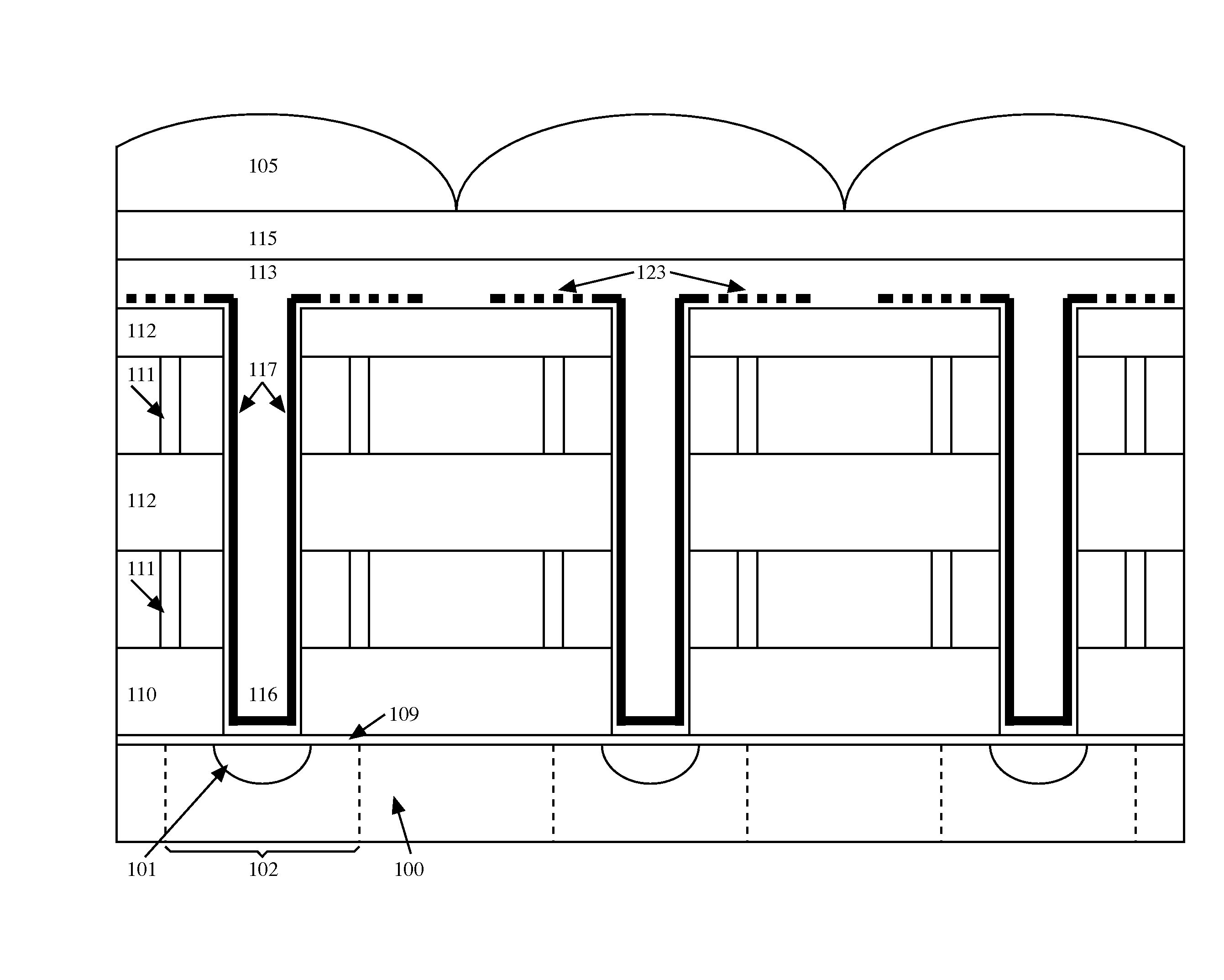
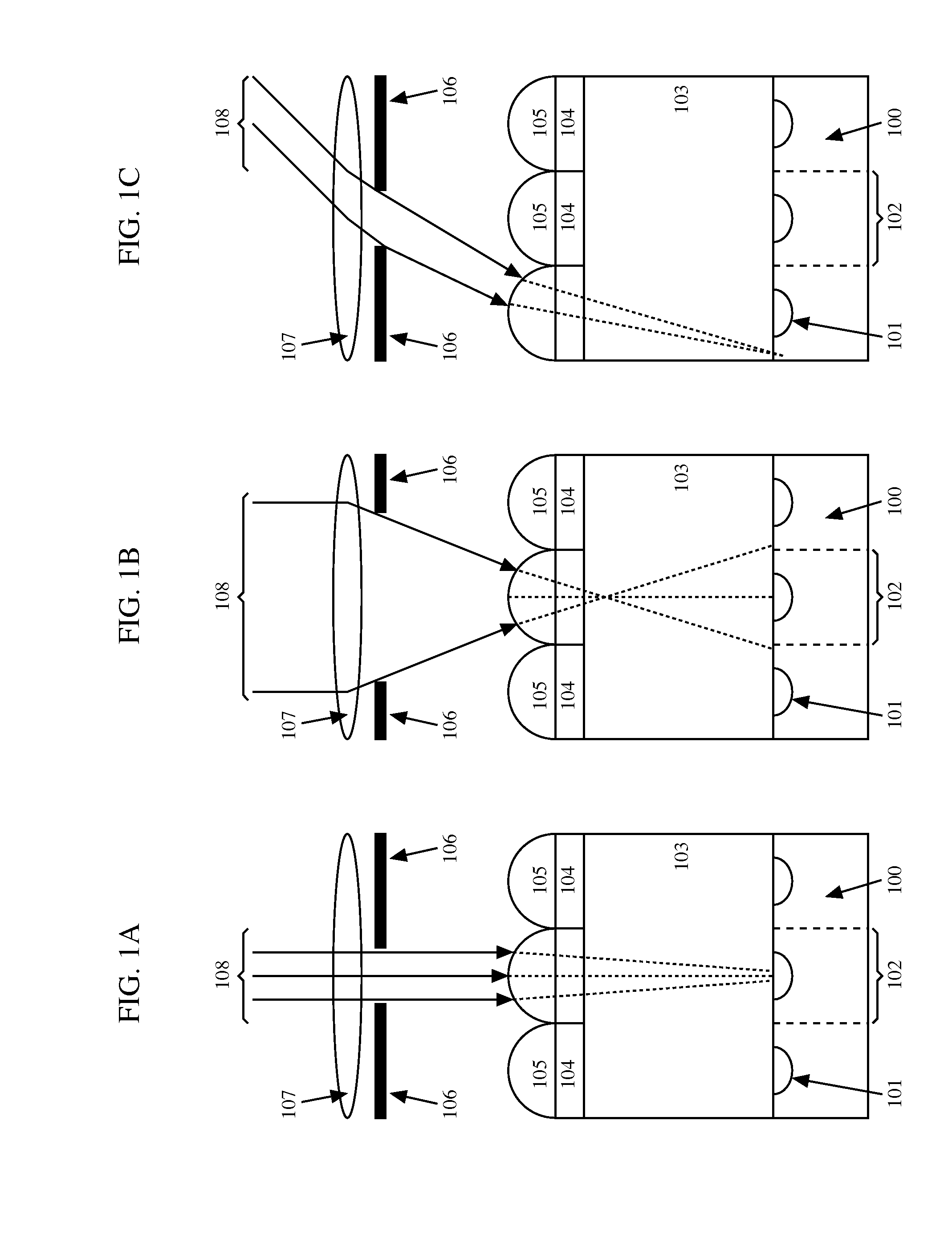
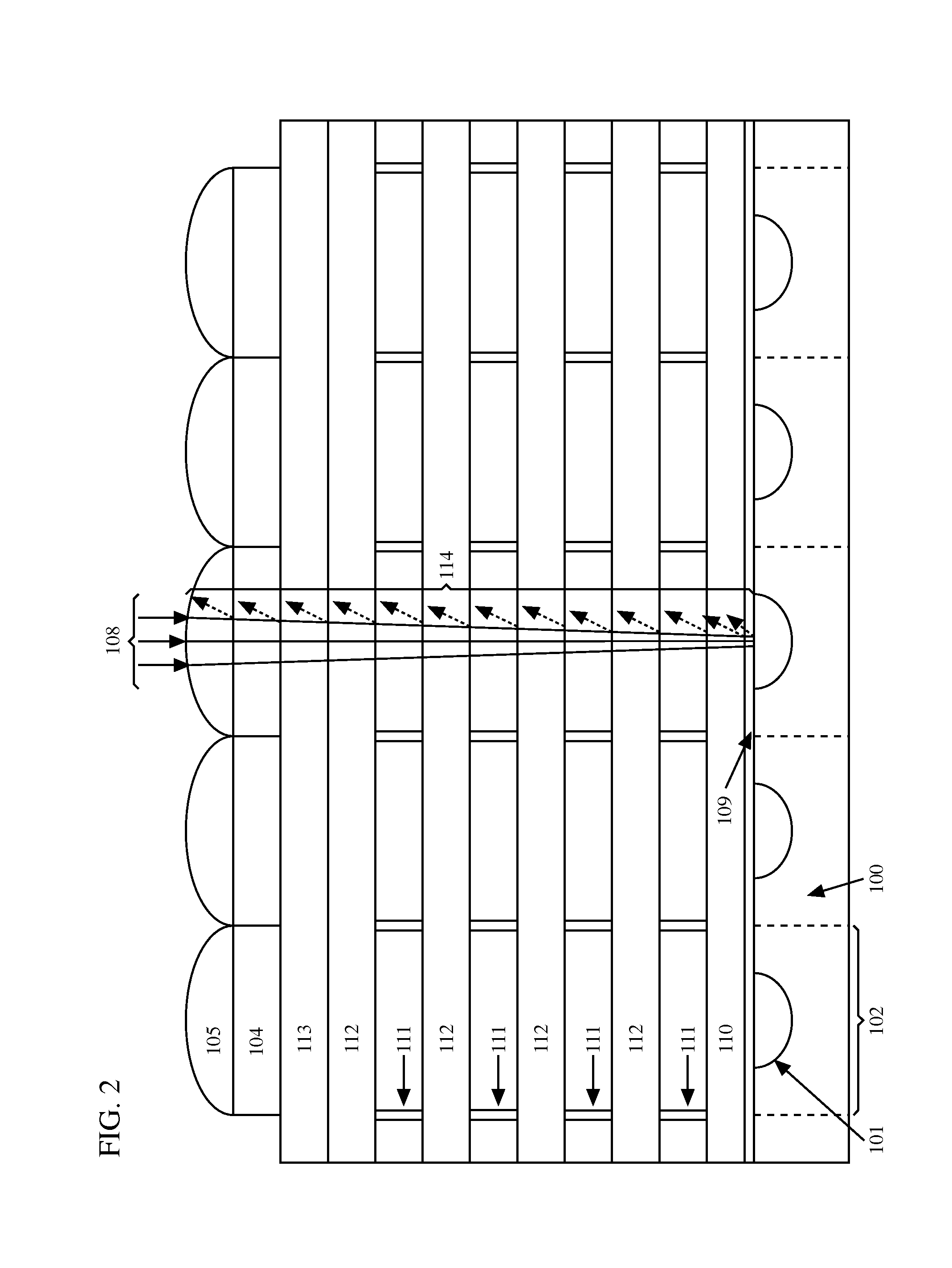
[0056]100—Substrate.[0057]101—Photo-diode.[0058]102—Pixel.[0059]103—Metallization stack.[0060]104—Color filters.[0061]105—Microlenses.[0062]106—Iris.[0063]107—Lens.[0064]108—Light rays.[0065]109—Dielectric barrier film (for example silicon nitride).[0066]110—Pre-metal dielectric (typically silicon oxide).[0067]111—Metal lines.[0068]112—Inter-metal dielectric.[0069]113—Passivation layer.[0070]114—Reflected light rays.[0071]115—Layer with Graded Index of Refraction (graded in the vertical direction-direction of deposition).[0072]116—High Index of Refraction material, for example silicon nitride or diamond.[0073]117—Metal.[0074]118—First width of Light-Tunnels.[0075]119—Second width of Light-Tunnels.[0076]120—Third width of Light-Tunnel[0077]121—Representation of a Surface Plasmon-Polariton at the surface of a metal layer.[0078]122—Inverted truncated cone or pyramid geometry with radially graded index of refraction (forming a GRIN lens).[0079]123—Perforate...


PUM


Abstract

Photonic passive structure to couple and guide light between photonic active devices (101), such as photo-diodes, light emitting devices and light-valves, which may be arranged into 2D arrays, and the top of the metallization layer stack (110,111,112) interconnecting said devices, with said photonic passive structure comprising a hole (116) between the near surface of said photonic active Ndevices and the top of said metallization stack, said hole being filled with a dielectric (113) having embedded metal films (117) and in which the embedded metal thin films are connected to a planar perforated metal film (123,124) formed on top of the metallization stack.

Description

BACKGROUND OF THE INVENTION[0001]The present invention relates to the coupling of light between a pixel comprising a light-sensor, and / or a light-emitter, and / or a light-valve, and other optical elements such as wavelength filters, polarization filters, beam splitters, etc. Such optical elements can be implemented with a varied set of technologies, including refractive optics, diffractive optics, 1D, 2D or 3D photonic crystals (or photonic band-gap materials), including purely dielectric structures, and / or metallodielectric structures, and / or metal structures with the possibility of using surface plasmon-polariton (SPP) effects.[0002]Standard image sensors have microlens arrays, also referred to as microlenticular arrays or lenslet arrays, to focus the incoming light rays into the photo-diode region of each pixel, which in certain types of CCDs and in all types of CMOS Image Sensors (CIS) is only a fraction of the size of the total pixel. The ratio of the area of the light-sensing r...

Claims


Application Information

Patent Timeline
IPC IPC(8): G02B6/122B05D5/06B29D11/00
CPCG02B6/08G02B6/12G02B6/4249G02B6/4298G02B6/43H01L27/14621G02B2006/12176H01L27/14685H01L31/0232H01L27/14629G02B6/1225G02B2006/12166H01L27/14636
Inventor AUGUSTO, CARLOS J.R.P.
Owner QUANTUM SEMICON
Why Eureka
Try Eureka