Photonic use of intermediate band materials on a chalcogenide-type semiconductor

Inactive Publication Date: 2010-08-19
UNIV MADRID POLITECNICA +1
View PDF0 Cites 8 Cited by
  • Summary
  • Abstract
  • Description
  • Claims
  • Application Information

AI Technical Summary

Benefits of technology

[0013]Another more preferred aspect of the invention is the use in the manufacturing of mat

Problems solved by technology

When this phenomenon is desired to be used to convert the sun's radiating energy into electrical energy, the overall efficiency of the energy conversion is limited, due to the spectral characteristics of the solar radiation; the theoretical limit is 40.7% in said devices (with a single photon absorption material).
1734], al

Method used


Image

  • Photonic use of intermediate band materials on a chalcogenide-type semiconductor
  • Photonic use of intermediate band materials on a chalcogenide-type semiconductor
  • Photonic use of intermediate band materials on a chalcogenide-type semiconductor

Examples


Example

Example 1

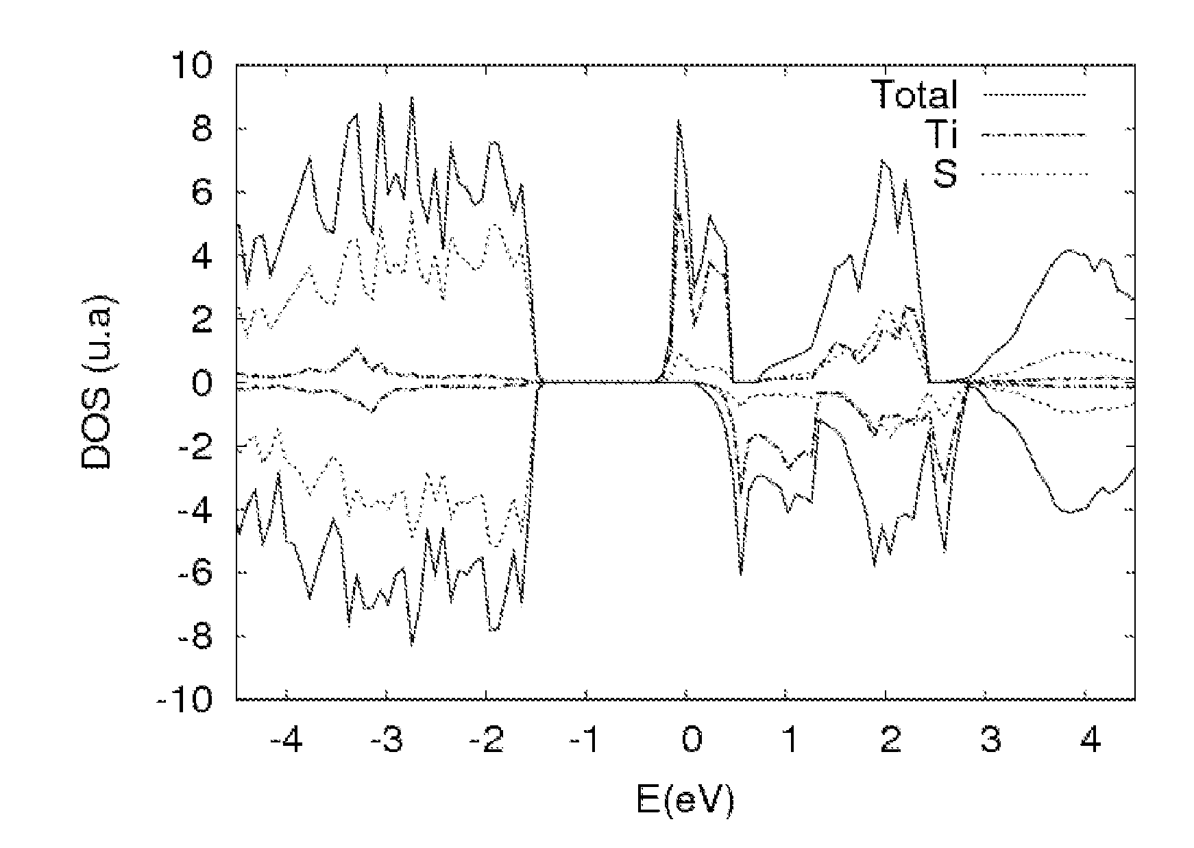
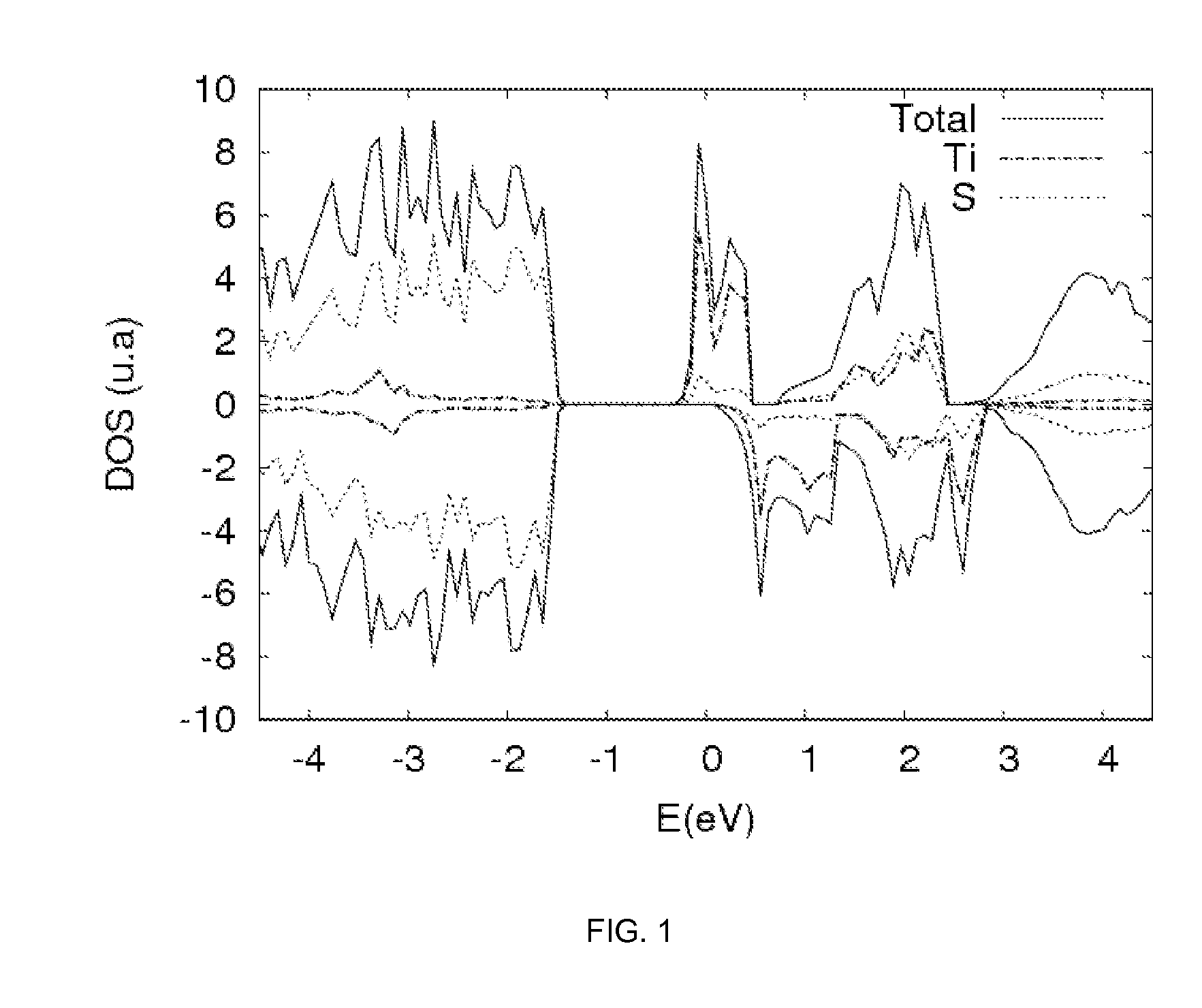
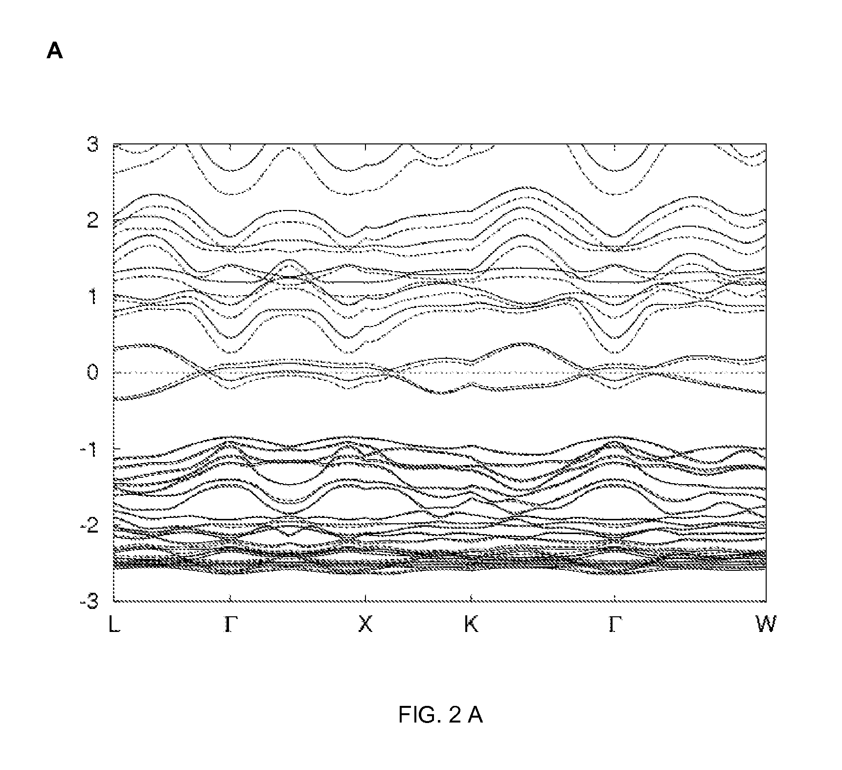
[0041]Determination of the intermediate band electronic structure in sulfides with spinel-type structure which comprise indium in octahedral position and wherein part thereof has been substituted by titanium or vanadium.

[0042]The authors of this invention performed quantum mechanics calculations using the standard methodology of the density functional theory (DFT), in its generalized gradient approximation (GGA). For this, the VASP program was used [G. Kresse and J. Hafner, Phys. Rev. B 47 (1993) RC558; G. Kresse and J. Furthmüller, Phys. Rev. B 54 (1996) 11169; G. Kresse and J. Joubert, Phys. Rev. B 59 (1999) 1758], based on an expansion of the electronic functions in flat waves and representing the internal elections with PAW potentials. A calculation was made on the direct spinel structure of the compound MgIn2S4 (which has an experimental bandgap width of approx. 2.4 eV and constitutes for the purposes of this invention a satisfactory model of the In chalcogenides with...

Example

Example 2

Preparation of Indium Sulfide Substituted in Part with Vanadium

[0047]As demonstration that materials of this type can be obtained with an electronic structure in accordance with that predicted by calculations, we should indicate that the preparation of an indium sulphide substituted by vanadium was undertaken. A solvothermal method was used, verifying, in first place, that In2S3 could be obtained, using the reaction

2InCl3+3Na2S→In2S3+6NaCl

[0048]The reaction was carried out by heating in an autoclave with Teflon coating an aqueous solution of both reagents during 16 h at temperatures of up to 150° C. The characteristics (x-ray diffraction diagram, light absorption spectrum) of the solid product obtained in the form of yellowish polycrystalline powder indicated that this material was effectively achieved. Next, the same reaction was carried out by substituting 10% of InCl3 by VCl3. In this case, the solution was prepared in the absence of air, using a water-ethylene glycol m...


PUM


Abstract

The invention relates to the use, in the manufacturing of materials or devices for photonic applications, of chalcogenide-type compounds having an octahedrally coordinated indium element and wherein a transition element is introduced in octahedral position generating a partially occupied intermediate band separate from those of valence and conduction of the initial semiconductor, according to quantum mechanics calculations. This enables, by absorption of two photons having energy lower than the prohibited bandwidth of the initial semiconductor, a result equivalent to that achieved, without said intermediate band, by the absorption of a higher-energy photon. The use of such a material can thereby improve yield and performance of various photovoltaic, photocatalytic, photoelectrochemical, optoelectronic or photonic conversion devices. Indium sulfide substituted in part with vanadium or titanium is one of the specific materials having these properties that is synthesised according to the invention.

Description

FIELD OF THE ART[0001]The present invention relates to chalcogenide compounds which can function as intermediate band materials in photonic applications. Therefore, the invention is found within the sector of new materials, whilst its application is mainly located in the energy sector, and more specifically in the renewable energy sector, such as those which use solar photovoltaic panels or photocatalytic or photoelectrochemical light energy conversion systems; it can also be located, secondarily, in the information technologies sector, within the field of photonics, or the chemical and environmental protection industry, in particular in the applications based on photocatalytic and photoelectrochemical processes.STATE OF THE ART[0002]The photovoltaic devices for the use of solar energy most used in the state of the art are based on semiconductor materials whose electronic structure contains a valence band and a conduction band (which, in the absence of defects or doping elements are...

Claims


Application Information

Patent Timeline
IPC IPC(8): H01L31/042C01B17/00
CPCH01L21/02568H01L21/02628H01M14/005H01L31/0321H01L31/032H01L31/0328
Inventor CONESA CEGARRA, JOSE CARLOSLUCENA GARCIA, RAQUELWAHNON BENARROCH, PERLAPALACIOS CLEMENTE, PABLOFERNANDEZ SANCHEZ, JULIO JUANSANCHEZ NORIEGA, KEFRENAGUILERA BONET, IRENE
Owner UNIV MADRID POLITECNICA
Why Eureka
Try Eureka