Process for electrodeposition of copper chip to chip, chip to wafer and wafer to wafer interconnects in through-silicon vias (TSV)

a technology of through-silicon vias and copper, which is applied in the direction of electrolytic processes, solid-state devices, electrolysis components, etc., can solve the problems of wafer bending, explosive release of vapor, and various defects, so as to minimize stress, avoid defects, and maximize the electrodeposited filling of tsvs

Inactive Publication Date: 2010-08-19
ATOTECH DEUT GMBH
View PDF16 Cites 46 Cited by
  • Summary
  • Abstract
  • Description
  • Claims
  • Application Information

AI Technical Summary

Benefits of technology

[0007]In various of its embodiments, the present invention avoids the disadvantages of known processes and, more particularly, maximizes the electrodeposited filling of the TSVs with

Problems solved by technology

TSVs have been used for forming electrical connections between respective layers in a stacked or 3D arrangement in devices such as MEMS and semiconductor devices, but have suffered from various defects arising, at least partially, from difficulty in electroplating highly pure copper into the very large, high aspect ratio vias in the TSVs.
Attempts to electrodeposit high purity copper into such high aspect ratio TSVs have been partially successful, but have been plagued with problems arising from (a) internal stresses in the copper deposit which can result in wafer bending or deformation upon subsequent heating, (b) non-uniform deposits (i.e., grain boundaries, crystal structure defects, etc.), (c) inclu

Method used


Image

  • Process for electrodeposition of copper chip to chip, chip to wafer and wafer to wafer interconnects in through-silicon vias (TSV)
  • Process for electrodeposition of copper chip to chip, chip to wafer and wafer to wafer interconnects in through-silicon vias (TSV)
  • Process for electrodeposition of copper chip to chip, chip to wafer and wafer to wafer interconnects in through-silicon vias (TSV)

Examples


example 1

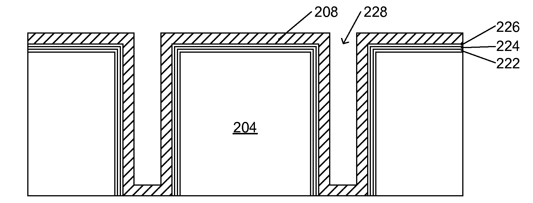
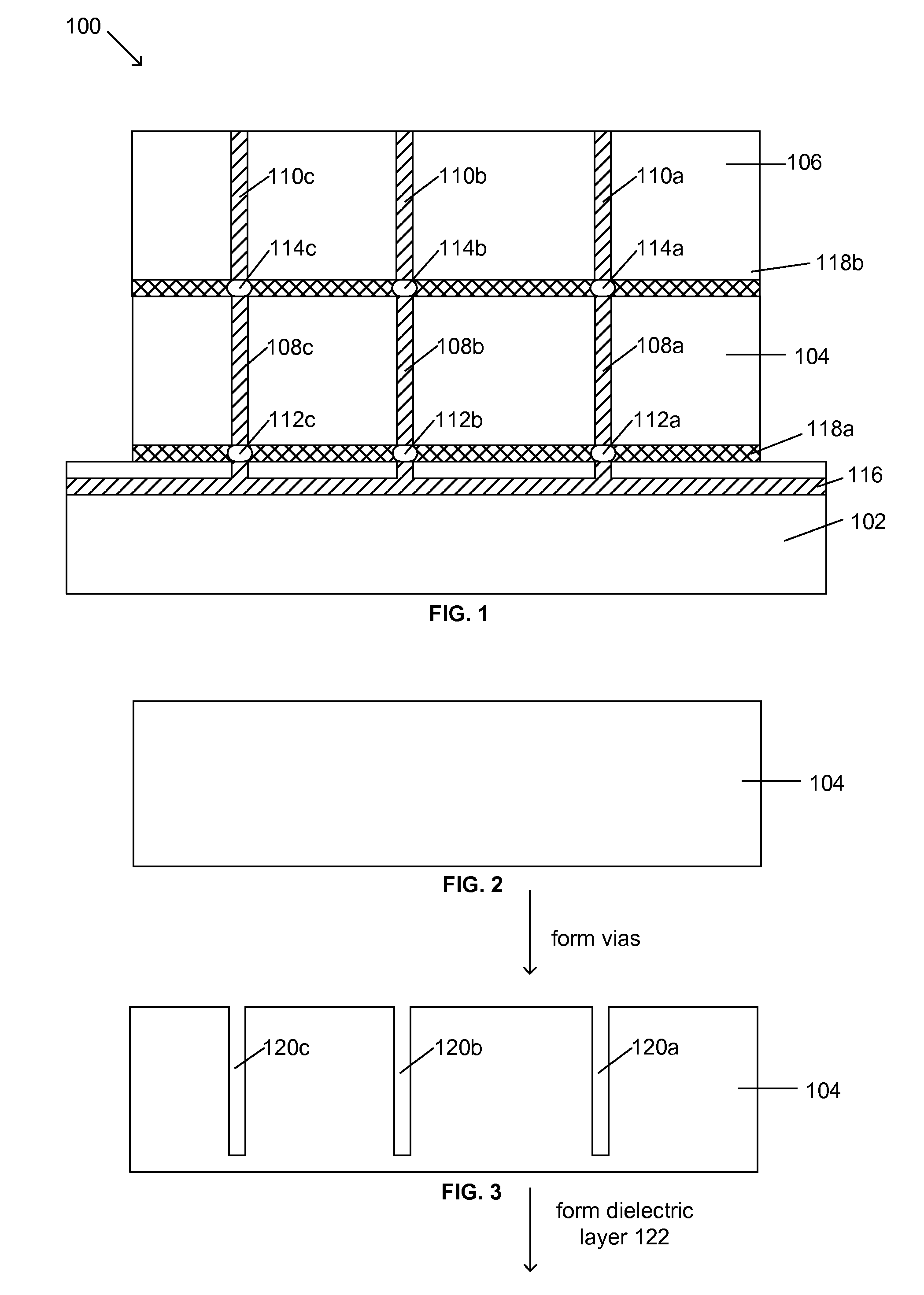
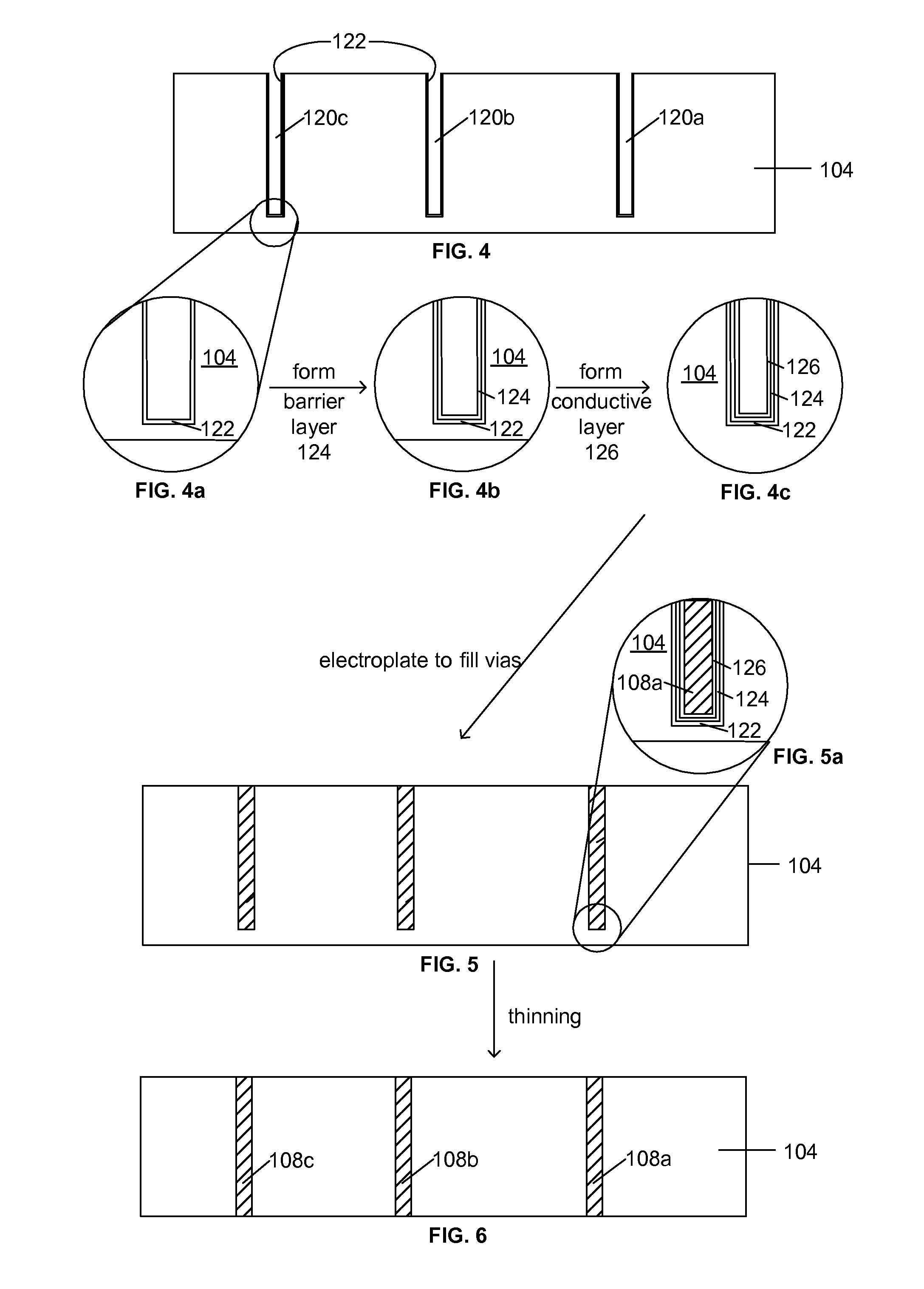
[0161]To produce a TSV filled with a high purity copper deposit, a wafer is provided with vias having a diameter of about 10 microns and a depth of about 50 microns. The vias are initially coated with a dielectric layer of silicon dioxide formed by high temperature oxidation of the inner sidewalls of the vias. The dielectric layer on the inner sidewalls of the vias is next coated with a diffusion barrier layer formed from tantalum nitride applied by sputtering. Subsequently, the diffusion barrier layer is coated with a copper base metal layer by a sputtering process, in which the copper base metal layer has a thickness of about 0.1 micron. The wafer is then immersed in a copper deposition bath described below in which the wafer is connected as a cathode and an insoluble anode is included. The via is filled with high purity copper by electrodeposition from the bath having the following ingredients, to form the TSVs in accordance with the present invention:

H2SO4, 98% by wt.130 g / lCuSO...

example 2

[0167]Copper stress in TSVs deposited by different plating methods using the above-disclosed bath in accordance with the invention and either using a similar bath without the added Fe2+ / Fe3+ ions or using a similar bath but with a soluble copper anode, in which pulsed current is applied with the parameters shown in the table below:

Pulse inmillisecondsPhaseIforward / IreverseForward- / Pulse-gap inshift inExamplesin A / dm2Reverse-Pulsemillisecondsdegrees1 and 26 / 4072 / 44180

Electrodeposition MethodStressSoluble Copper Anode:163.2 ± 34.3 MPa(prior art)Soluble Copper Anode w / Fe2+ / Fe3+ redox113.4 ± 40.1 MPa(prior art)Inert Anode w / Cu / Cu2+ / Fe2+ / Fe3+ redox 66.9 ± 9.8 MPa(present invention)

[0168]The internal stress is measured as deposited without a post-annealing step. The measurement is via wafer warpage and bow (LASER measurement). The equipment used was a KLA-TENCOR FLX-2320 thin film stress measurement system, copper film thickness 1 micron, wafer thickness 750 micron.

[0169]As is clearly sho...


PUM

PropertyMeasurementUnit
Lengthaaaaaaaaaa
Lengthaaaaaaaaaa
Lengthaaaaaaaaaa

Abstract

A process of electrodepositing high purity copper in a via in a silicon substrate to form a through-silicon-via (TSV), including immersing the silicon substrate into an electrolytic bath in an electrolytic copper plating system in which the electrolytic bath includes an acid, a source of copper ions, a source of ferrous and/or ferric ions, and at least one additive for controlling physical-mechanical properties of deposited copper; and applying an electrical voltage for a time sufficient to electrodeposit high purity copper to form a TSV, in which a Fe+2/Fe+3 redox system is established in the bath to provide additional copper ions to be electrodeposited by dissolving copper ions from a source of copper metal.

Description

BACKGROUND[0001]1. Field of the Invention[0002]The invention relates to a process of electrolytically forming conductor structures from highly pure copper, more specifically to electrolytically forming conductor structures from highly pure copper in through-silicon vias (TSVs) when producing devices such as MEMS or semiconductor devices. Such TSVs are useful, e.g., in integrated circuits, in a stacked or 3D arrangement, in which the TSV provide electrical connection between the respective layers of the device, where the TSV have relatively large diameter, relatively great depth and a high aspect ratio.[0003]2. Description of Related Art[0004]The demands of fabricating cheaper, smaller and lighter electronic products offering better performance and increased functionality are continuously growing. The number of electronic device on a single chip is still rapidly increasing, and the ability of 2D layouts to accommodate these demands is being exceeded. According to industry roadmaps, i...

Claims


Application Information

Patent Timeline
IPC IPC(8): C25D5/02C25D7/12
CPCC25D3/38C25D5/18C25D21/16C25D5/02H01L21/76898C25D7/123H01L21/2885H01L2224/131H01L2224/16145H01L2224/16245H01L2224/05573H01L2224/13025H01L2224/05647H01L2924/00014H01L2224/0554H01L24/03H01L24/05C25D5/617C25D5/611H01L2924/014H01L2224/05599H01L2224/0555H01L2224/0556
Inventor PREISSER, ROBERT F.
Owner ATOTECH DEUT GMBH
Why Eureka
Try Eureka