Photosensitive electrochromic device

a photosensitive electrochromic and electrochromic technology, applied in semiconductor devices, optics, instruments, etc., can solve the problems of inability to reduce the intrinsic layer the inability to reduce the thickness of silicon thin-film solar cells, and the inability to consume energy. achieve the effect of reducing fabrication costs and time, and facilitating mass production

Active Publication Date: 2010-08-19
IND TECH RES INST
View PDF7 Cites 14 Cited by
  • Summary
  • Abstract
  • Description
  • Claims
  • Application Information

AI Technical Summary

Benefits of technology

[0017]Based on the above, the photosensitive electrochromic device of the present invention adopts the following design: the monolithic series-connected thin-film solar cell module is used to drive the electrochromic solution, wherein an anode layer and a cathode layer of the thin-film solar cell module are deposited on one transparent substrate, so as to form the anode and the cathode of the photosensitive electrochromic device on the same surface. When sunlight irradiates the thin-film solar cell module, the module directly produces current that induces redox reaction to occur in the el...

Problems solved by technology

A regular electrochromic device may serve as a smart window for power saving and be used in green buildings, but it still requires an electric energy source, which consumes energy.
However, to apply a typical structure like this in practice, many problems need to be solved, for example, the stability of the employed photosensitive layer or the feasibility of enlarging the area of the device.
However, the inorganic electrochromic material intrinsically requires a high driving voltage and a high charge density for working, and thus the th...

Method used


Image

  • Photosensitive electrochromic device
  • Photosensitive electrochromic device
  • Photosensitive electrochromic device

Examples


first embodiment

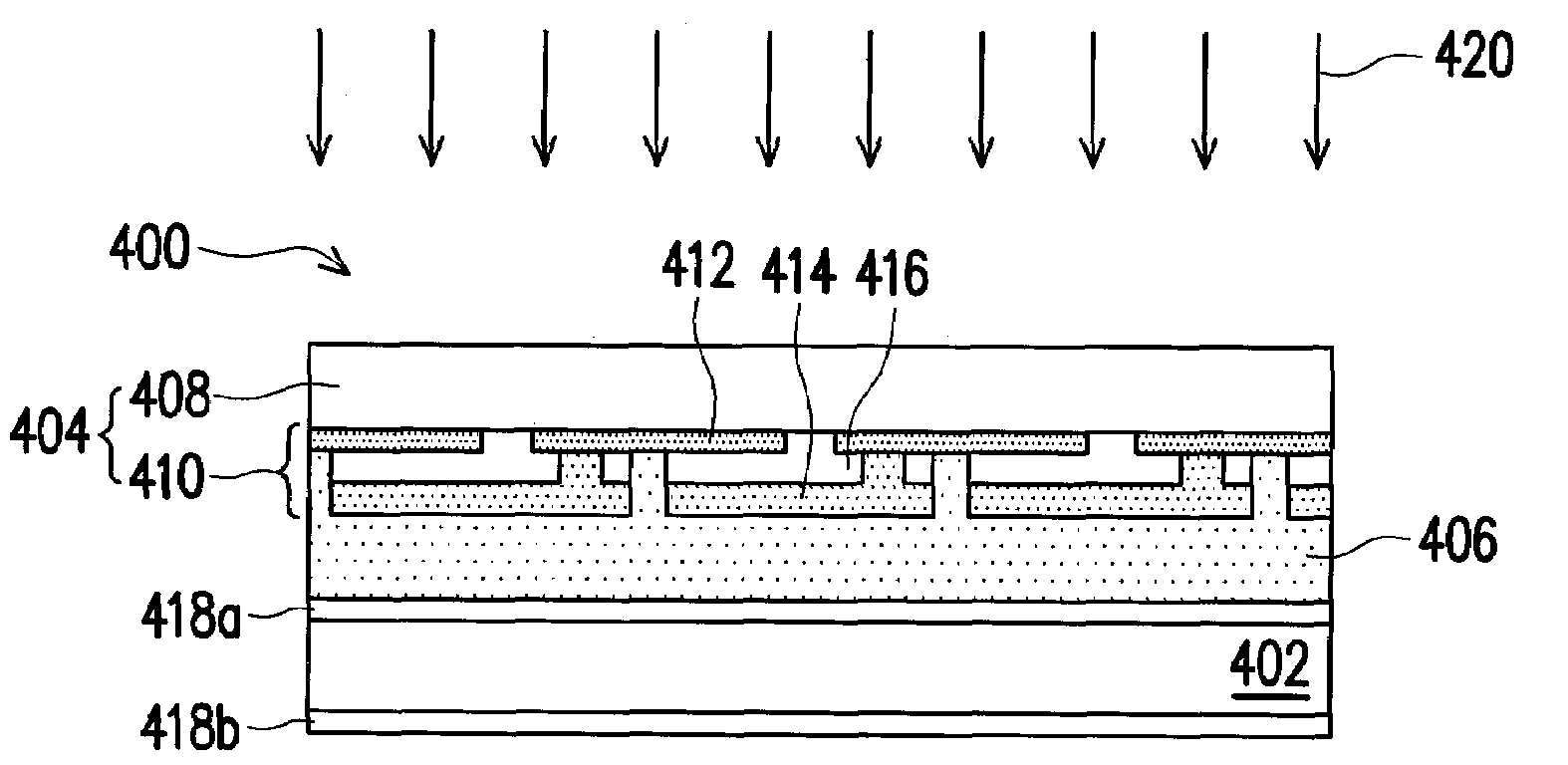
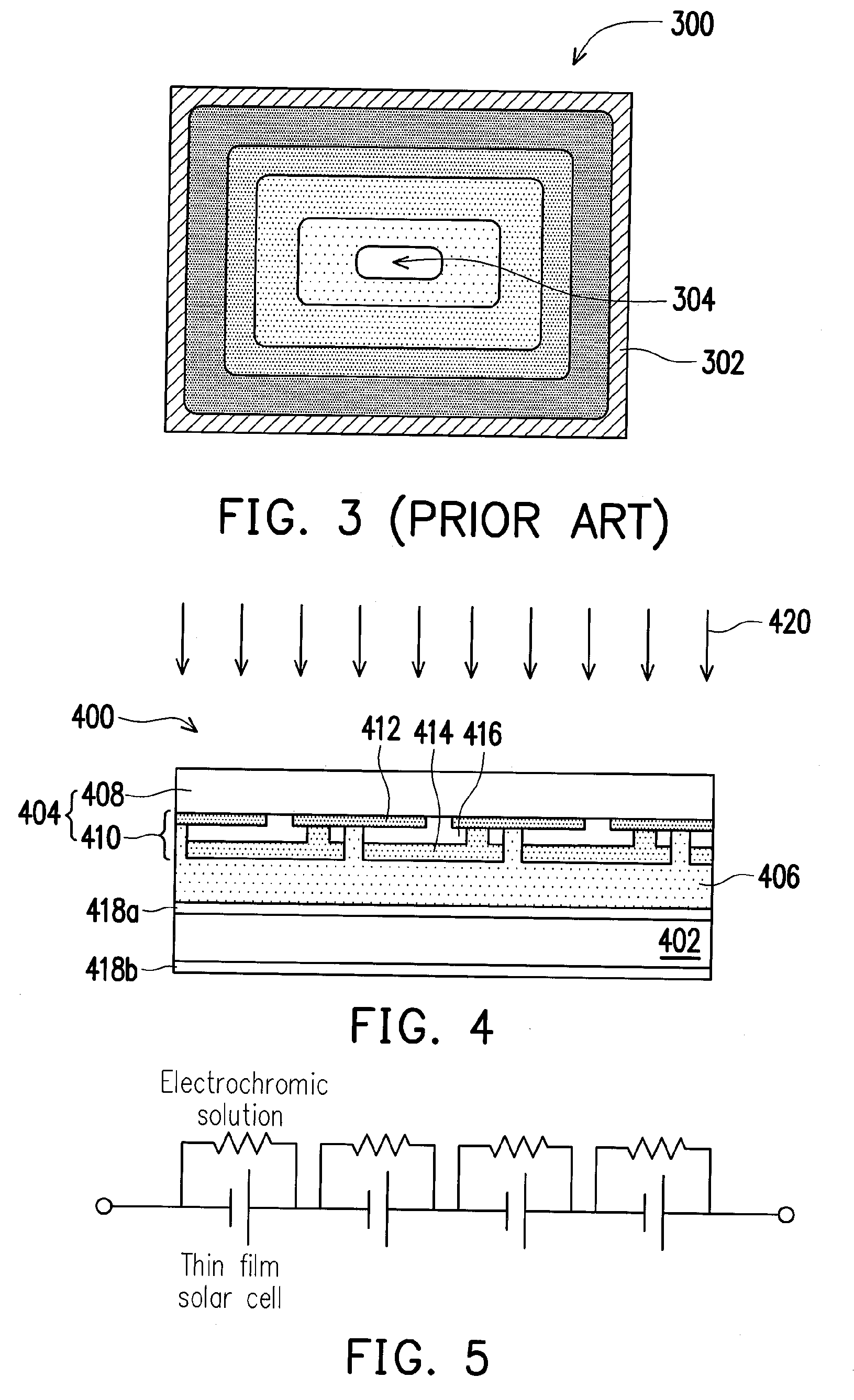
[0039]In the first embodiment, the transparent non-conductive substrate 402 is, for example, glass, plastic or other appropriate flexible substrates. A material of the transparent substrate 408 of the thin-film solar cell module 404 is, for example, glass, plastic or a flexible substrate. A composition of the electrochromic solution 406 is, for example, at least one redox-type organic small molecule electrochromic material and at least one solvent, wherein the redox-type organic small molecule electrochromic material is one selected from the group consisting of cathodic electrochromic material, anodic electrochromic material, and a combination thereof. The above-mentioned cathodic electrochromic material is, for example, methyl viologen, ethyl viologen, heptyl viologen (HV), benzyl viologen or propyl viologen; the anodic electrochromic material is, for example, dimethylphenazine, phenylene diamine or TMPD (N,N′,N,N′-tetramethyl-p-phenylenediamine) and the redox potential of the elec...

second embodiment

[0042]FIGS. 6A-6E are cross-sectional diagrams illustrating a process flow of fabricating a photosensitive electrochromic device according to the present invention.

[0043]Referring to FIG. 6A first, by conducting the step of FIG. 6A, a TCO thin film is formed on the transparent substrate 600. Then, a first laser scribing process is performed to remove the TCO thin film within the areas P1 so as to form a plurality of anode layers 602.

[0044]Next referring to FIG. 6B, a plasma-enhanced chemical vapor deposition (PECVD) process is performed to implement continuous deposited film on the transparent substrate 600 and the anode layers 602 so as to form the semiconductor thin film 604, and then a second laser scribing process is performed to remove a portions of the semiconductor thin film 604 that is within the areas P2 and the semiconductor thin film 604 is separated into a plurality of semiconductor thin films 604.

[0045]Referring to FIG. 6C, a physical vapor deposition (PVD) process is p...


PUM


Abstract

A photosensitive electrochromic device includes a transparent non-conductive substrate, a thin-film solar cell module and an electrochromic solution. The thin-film solar cell module is a monolithic series-connected module and includes a transparent substrate and a plurality of thin-film solar cells located on the transparent substrate, wherein all the thin-film solar cells in the thin-film solar cell module are connected in series, and the above-mentioned electrochromic solution is located between the transparent non-conductive substrate and the thin-film solar cell module.

Description

CROSS-REFERENCE TO RELATED APPLICATION[0001]This application claims the priority benefit of Taiwan application serial no. 98104654, filed Feb. 13, 2009. The entirety of the above-mentioned patent application is hereby incorporated by reference herein and made a part of specification.BACKGROUND OF THE INVENTION[0002]1. Field of the Invention[0003]The present invention generally relates to a photosensitive electrochromic device.[0004]2. Description of Related Art[0005]A regular electrochromic device may serve as a smart window for power saving and be used in green buildings, but it still requires an electric energy source, which consumes energy. Typical electrochromic devices are categorized into a solid type and a liquid type. A solid electrochromic device has a structure as shown in FIG. 1, where an upper layer and a lower layer of an electrochromic device 100 are respectively formed by a glass / plastic transparent substrate 102. There are at least five coated / deposited layers with d...

Claims


Application Information

Patent Timeline
IPC IPC(8): G02F1/163G02F1/157
CPCG02F1/1521G02F2001/1512G02F2001/13324G02F1/163G02F1/1503G02F2001/15145G02F1/13324
Inventor HUANG, LEE-MAYCHEN, CHUN-HENG
Owner IND TECH RES INST
Why Eureka
Try Eureka