

Electron emitting element, electron emitting device, light emitting device, image display device, air blowing device, cooling device, charging device, image forming apparatus, electron-beam curing device, and method for producing electron emitting element
- Summary
- Abstract
- Description
- Claims
- Application Information
AI Technical Summary
Benefits of technology
Problems solved by technology
Method used
Image

Examples
embodiment 1
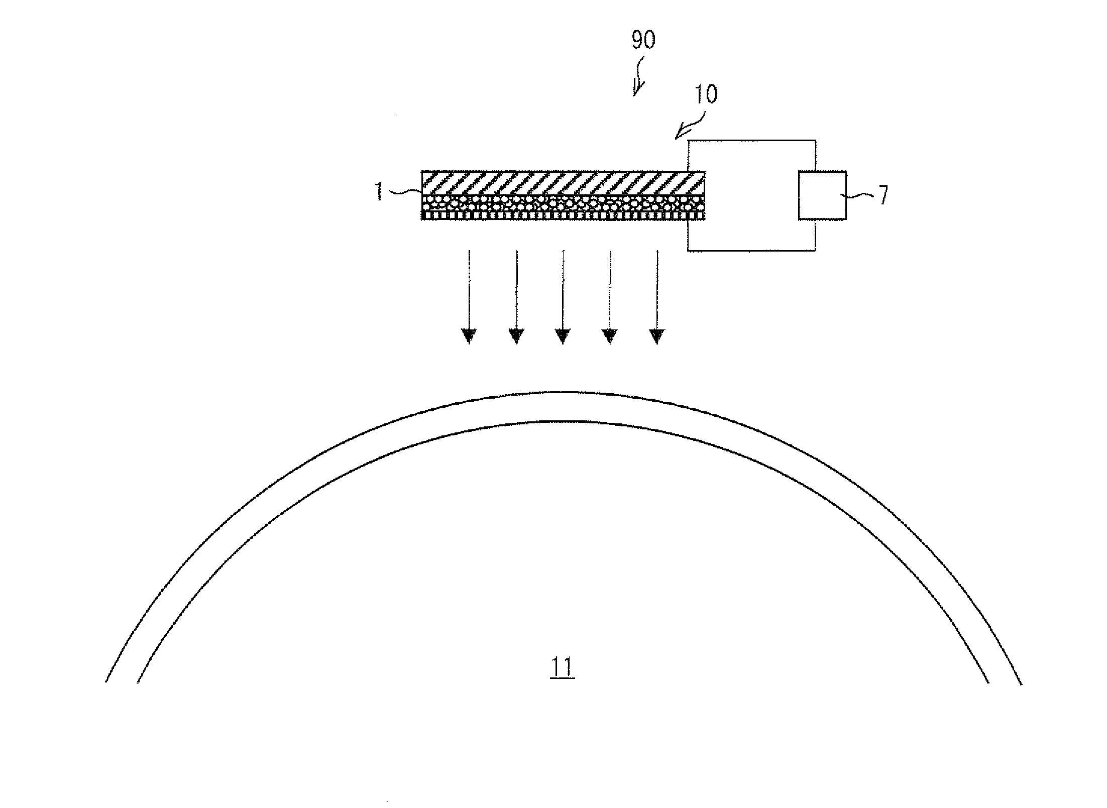
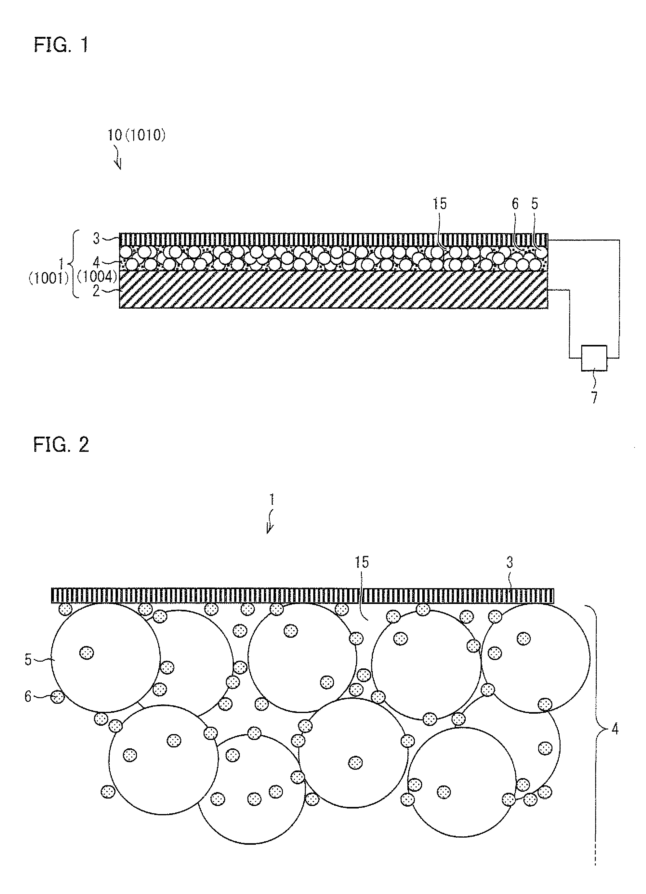
[0066]FIG. 1 is a schematic view illustrating an embodiment of an electron emitting device including an electron emitting element of the present invention. As illustrated in FIG. 1, an electron emitting element 1 of the present embodiment includes an electrode substrate 2 serving as a lower electrode, a thin-film electrode 3 serving as an upper electrode, and an electron acceleration layer 4 sandwiched between the electrode substrate 2 and the thin-film electrode 3. Further, the electrode substrate 2 and the thin-film electrode 3 are connected to a power supply 7, so that a voltage can be applied between the electrode substrate 2 and the thin-film electrode 3 which are provided so as to face each other. The electron emitting element 1 applies a voltage between the electrode substrate 2 and the thin-film electrode 3 so that current flows between the electrode substrate 2 and the thin-film electrode 3, that is, in the electron acceleration layer 4. A part of electrons in the current a...
example 1
[0093]The following explains an experiment in which current measurement was carried, out by use of electron emitting elements according to Embodiment 1. Note that this experiment is merely an example of the present embodiment and by no means limits the present invention.
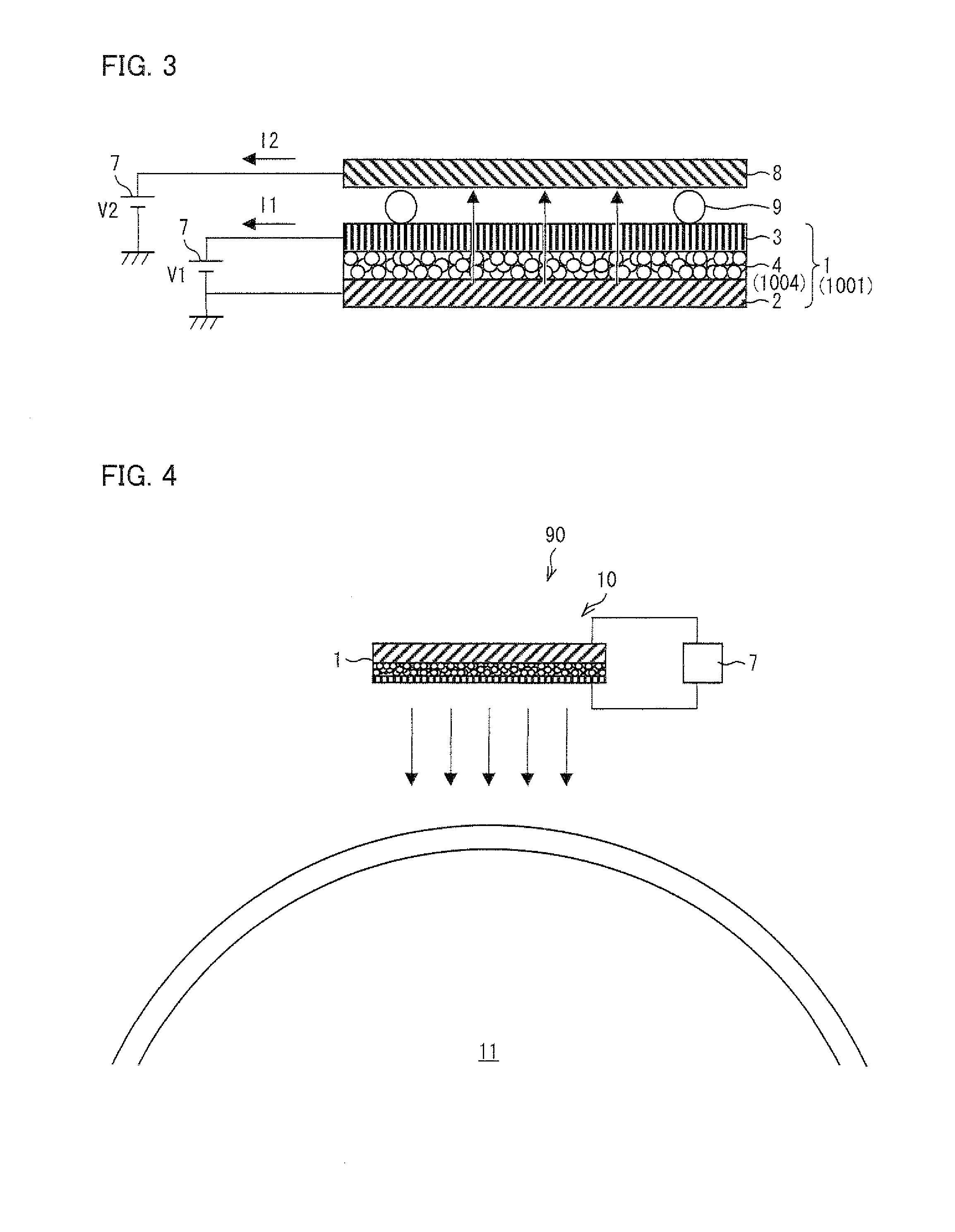
[0094]First, electron emitting elements of Examples 1-1 to 1-4 were produced as described below. Then, an experiment was carried out on the electron emitting elements of Examples 1-1 to 1-4. In the experiment, electron emission current per unit area was measured by using an experiment system as shown in FIG. 3. In the experiment system of FIG. 3, a counter electrode 8 was provided on a side of the thin-film electrode 3 of the electron emitting element 1 so that the counter electrode 8 and the thin-film electrode 3 sandwiched an insulating spacer 9. Each of the electron emitting element 1 and the counter electrode 8 was connected to a power supply 7 so that a voltage V1 was applied to the electron emitting element 1 a...
example 1-1
[0095]First, 2.0 g of ethanol solvent and 0.5 g of tetramethoxysilane KBM-04 (manufactured by Shin-Etsu Chemical Co., Ltd.) were supplied into a 10 mL reagent bottle, and then 0.5 g of spherical silica particles AEROSIL R8200 (manufactured by Evonik Degussa Japan Co., Ltd., average particle diameter: 12 nm) were added as the insulating material 5. The reagent bottle was then set in an ultrasonic dispersion device so that an insulating material-containing resin binder dispersion solution A was prepared. A content of the insulating material in the dispersion solution A was 17% by weight.
[0096]Next, the dispersion solution A obtained as described above and a conductive fine particle solution containing the conductive fine particles 6 were mixed. The conductive fine particle solution containing the conductive fine particles 6 used in the present example was a silver nanoparticle-containing hexane dispersion solution (manufactured by Applied Nano Particle Laboratory Co., average particle...
PUM
 Abstract
Description
Claims
Application Information