High Throughput Multi-Wafer Epitaxial Reactor

a multi-wafer, epitaxial technology, applied in the direction of solid-state diffusion coating, crystal growth process, polycrystalline material growth, etc., can solve the problems of wafer warpage, poor uniformity, low throughput, etc., to enhance the uniformity of film deposition, simplify the reactor chamber, and enhance the effect of deposition uniformity

Active Publication Date: 2010-08-26
SVAGOS TECHNICK INC
View PDF8 Cites 23 Cited by
  • Summary
  • Abstract
  • Description
  • Claims
  • Application Information

AI Technical Summary

Benefits of technology

[0012]The present invention provides an improved design for an epitaxial reactor with higher throughput, a wafer sleeve containing a multiplicity of wafers within a small reaction volume to improve usage of process gases and minimize unwanted deposition on the reaction chamber walls, and increased lamp lifetimes through improved lamp temperature control. A high degree of control over film thickness and resistivity uniformities within and between wafers may be achieved in the present invention without the need for rotary or other types of wafer motion during the deposition process, thereby simplifying the design of the reactor chamber. The epitaxial reactor of the present invention may comprise one or more lamp modules which irradiate a wafer sleeve contained within a reactor frame which also supports the lamp modules. Alternative embodiments of the present invention may employ either resistive heating or inductive heating of the wafer sleeve, instead of radiant lamp heating.
[0015]The process gases for epitaxial deposition may be fed directly into the interior space of the wafer sleeve by a set of process gas inlet tubes on the top and bottom of the reactor frame. Also on the top of the reactor frame is a set of purge gas inlet tubes, typically supplying hydrogen gas into the volume within the reactor frame, but outside of the wafer sleeve. Thus, a minimum amount of purge gas is introduced into the outer portions of the reactor module, thereby minimizing the amount of undesirable deposition on surfaces outside of the interior of the reactor module. Deposition on the inner surfaces of the reactor module is further reduced by water cooling of the reactor module. A set of exhaust outlet lines extends out of the top and bottom of the reactor frame. The exhaust gases comprise the purge gas, products from the epitaxial reaction within the reactor module, and unused reactant gases.
[0018]In a first embodiment of the overall system of the present invention, the epitaxial reactor may be integrated within a system comprising a preheat chamber, a single epitaxial deposition reactor, and a cool down chamber. In a second embodiment, two or more epitaxial deposition reactors may be employed in series, and combined with a preheat chamber and a cool down chamber. In this second embodiment, the epitaxial reactors each deposits part of the desired final film thickness. The wafer sleeve then moves to the next reactor for another partial deposition. For example, in a system comprising a preheat chamber, three epitaxial reactors, and a cool down chamber, each of the epitaxial reactors could deposit approximately one third of the final desired film thickness. During deposition within each of the three epitaxial reactors, the cross-flow deposition process could be employed to enhance deposition uniformity. Thus, the deposition time per epitaxial reactor would be one third that required for the single epitaxial reactor in the first embodiment. Assuming that the preheat and cool down times are less than one third of the total deposition time, this second embodiment could provide a wafer throughput roughly three times higher than the throughput of the first embodiment.
[0019]In a further embodiment of the present invention, a number of epitaxial reactors may be employed in series, with differing flow directions to achieve the desired overall film uniformity without the need for cross-flow processing within any of the epitaxial reactors. This approach, which may be combined with a preheat chamber and a cool down chamber, enables simpler reactor chambers to be employed since each reactor would need piping for only unidirectional process gas and exhaust flows.
[0020]Since the wafer sleeve of the present invention is heated by an array of lamps, a method of lamp sequencing may be employed to further enhance film deposition uniformities. In this method, the variation in deposition rate along a direction corresponding to the process gas flows may be made nearly linear by activation of the heating lamps for various duty cycles less than 100%, thereby controlling the deposition rate through real-time control of the wafer temperatures in different parts of the wafer sleeves. Combining lamp sequencing with cross-flow processing could then enable relatively uniform overall deposition rates to be obtained within and between wafers.

Problems solved by technology

Key disadvantages of this type of epitaxial reactor are low throughput, high gas consumption, wafer warpage, and worse uniformities than other types of prior art epitaxial reactors (see FIGS. 2 and 3).
Another important disadvantage is the need for frequent cleaning of the inner surfaces of the reactor chamber 101 due to unwanted deposition of films on these surfaces.
This unwanted deposition increases the cost of ownership due to higher process gas consumption and increased system downtime for maintenance and cleaning.
Some disadvantages are an inability to deposit dual layers and relatively high film resistivities.
However, an important disadvantage of this type of reactor is the high film costs for thicker films where the throughputs drop due to the longer epitaxial deposition times required.
Thus, the economics of semiconductor manufacturing may support relatively higher costs for each processing step than would be the case for other types of semiconductor products such as photovoltaic (PV) solar cell wafers.
Epitaxial deposition of a thin-film solar cell has the disadvantage that epitaxial deposition is typically a relatively slow process in achieving good epitaxy but the semiconducting light absorbing layers in a solar cell need to be relatively thick.

Method used


Image

  • High Throughput Multi-Wafer Epitaxial Reactor
  • High Throughput Multi-Wafer Epitaxial Reactor
  • High Throughput Multi-Wafer Epitaxial Reactor

Examples


Embodiment Construction

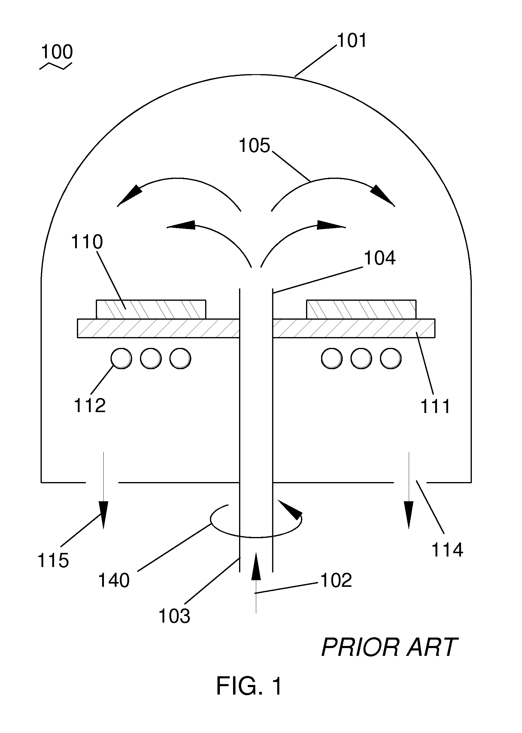
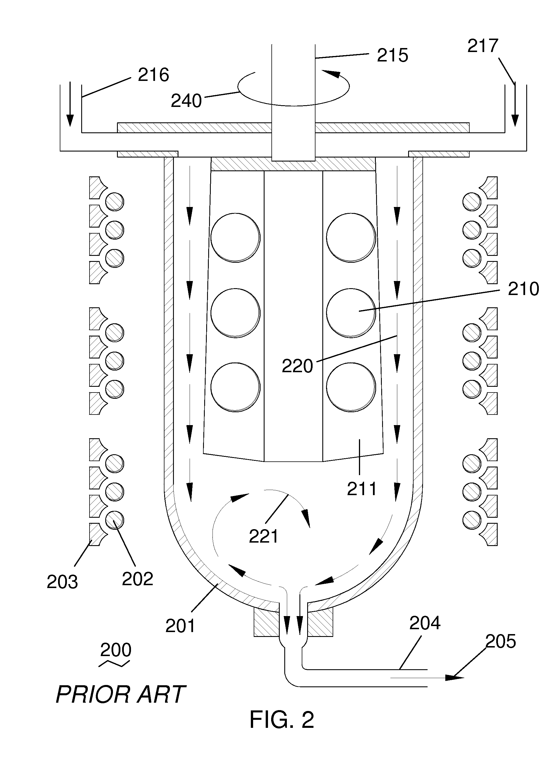
[0047]One disadvantage of prior art epitaxial deposition systems for PV cell applications is low throughput, measured in wafers per hour. Thus, it would be desirable for an epitaxial reactor to process a large number of wafers in parallel with the minimum deposition time practical to still achieve the desired properties in the deposited films on PV solar cell wafers.

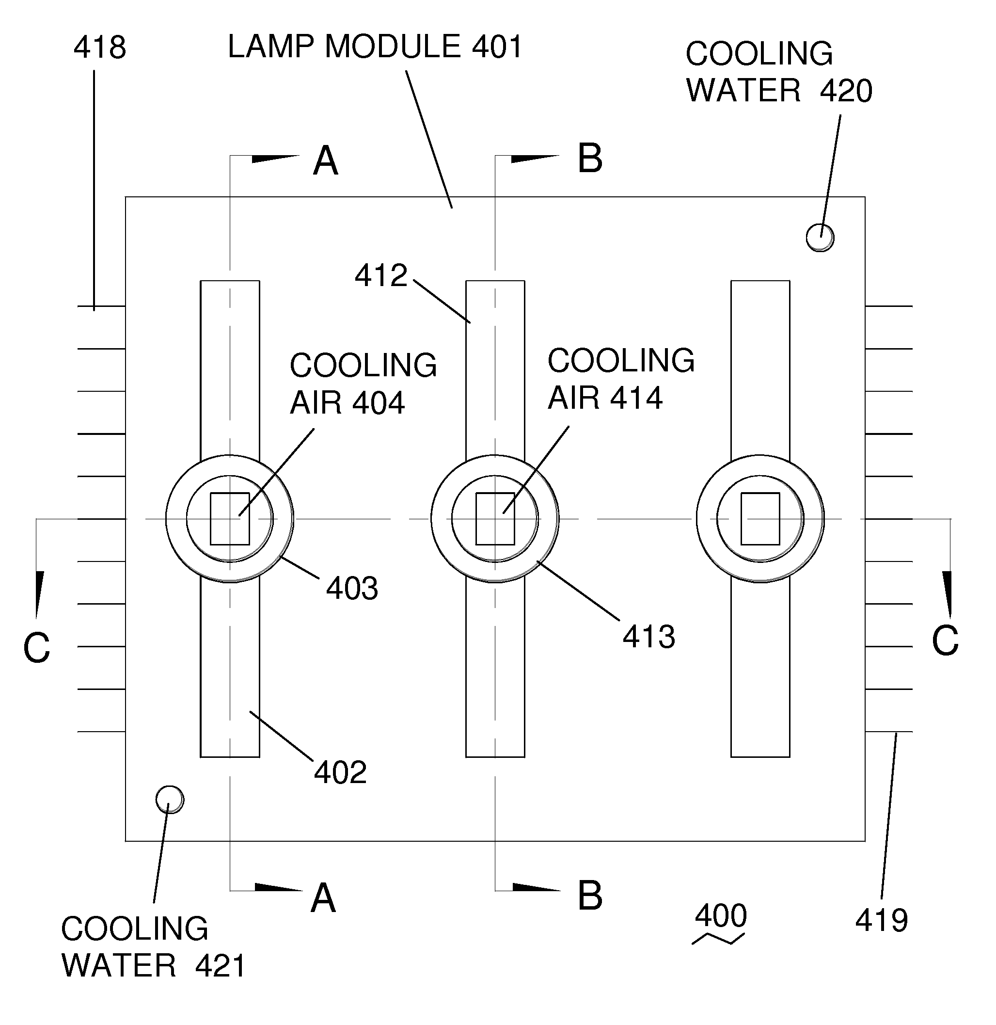
[0048]Accordingly, one aspect of the present invention includes an epitaxial reactor enabling the simultaneous deposition by chemical vapor deposition of films on a multiplicity of wafers, each supported by a carrier plate heated by an array of lamps mounted within a reflector assembly. The epitaxial reactor of the present invention comprises one or more lamp modules which illuminate a wafer sleeve contained within a reactor frame which also supports the lamp modules. The following figures describe the lamp module, wafer sleeve, and reactor frame separately. Next, the assembly of a reactor module is described, followed b...


PUM

PropertyMeasurementUnit
diameteraaaaaaaaaa
diameteraaaaaaaaaa
temperaturesaaaaaaaaaa

Abstract

An epitaxial reactor enabling simultaneous deposition of thin films on a multiplicity of wafers is disclosed. During deposition, a number of wafers are contained within a wafer sleeve comprising a number of wafer carrier plates spaced closely apart to minimize the process volume. Process gases flow preferentially into the interior volume of the wafer sleeve, which is heated by one or more lamp modules. Purge gases flow outside the wafer sleeve within a reactor chamber to minimize wall deposition. In addition, sequencing of the illumination of the individual lamps in the lamp module may further improve the linearity of variation in deposition rates within the wafer sleeve. To improve uniformity, the direction of process gas flow may be varied in a cross-flow configuration. Combining lamp sequencing with cross-flow processing in a multiple reactor system enables high throughput deposition with good film uniformities and efficient use of process gases.

Description

BACKGROUND OF THE INVENTION[0001]1. Field of the Invention[0002]This invention relates generally to the field of chemical vapor deposition (CVD) reactors for thin film deposition, especially of epitaxial films, and more particularly to CVD reactors employing one or more lamp-heated reactors and a travelling wafer sleeve exposed to the lamps, absorbing the lamp radiation, and mounting multiple wafers and defining process gas flow within the wafer sleeve.[0003]2. Description of the Related Art[0004]Epitaxial reactors for use in depositing thin films on wafers by chemical vapor deposition (CVD) may be categorized in terms of their method of heating the wafers, their overall arrangement of the wafers within the reaction chamber or chambers, and the overall tool architecture, including the number of reaction chambers and whether additional chambers for preheat and cool down are configured at the entrance and exit of the system, respectively. FIGS. 1-3 illustrate three different types of ...

Claims


Application Information

Patent Timeline
Patent Type & Authority Applications(United States)
IPC IPC(8): C23C16/56
CPCC23C16/4582C23C16/46C23C16/54C30B25/105C23C16/481C30B29/06C23C16/0209C23C16/455C23C16/463C30B25/12C23C16/00H01L21/205
Inventor SIVARAMAKRISHNAN, VISWESWARENSANGAM, KEDARNATHRAVI, TIRUNELVELI S.KASZUBA, ANDRZEJTRUONG, QUOC VINH
Owner SVAGOS TECHNICK INC
Why Eureka
Try Eureka