Photosensitive dry film resist, printed wiring board making use of the same, and process for producing printed wiring board
a technology of dry film resist and printed wiring board, which is applied in the direction of photosensitive materials, photomechanical equipment, instruments, etc., can solve the problems of insufficient heat resistance of solder, insufficient bonding strength at high temperature, and insufficient flexibility, etc., to achieve excellent flame retardancy, moisture resistance, and heat resistance. good
- Summary
- Abstract
- Description
- Claims
- Application Information
AI Technical Summary
Benefits of technology
Problems solved by technology
Method used
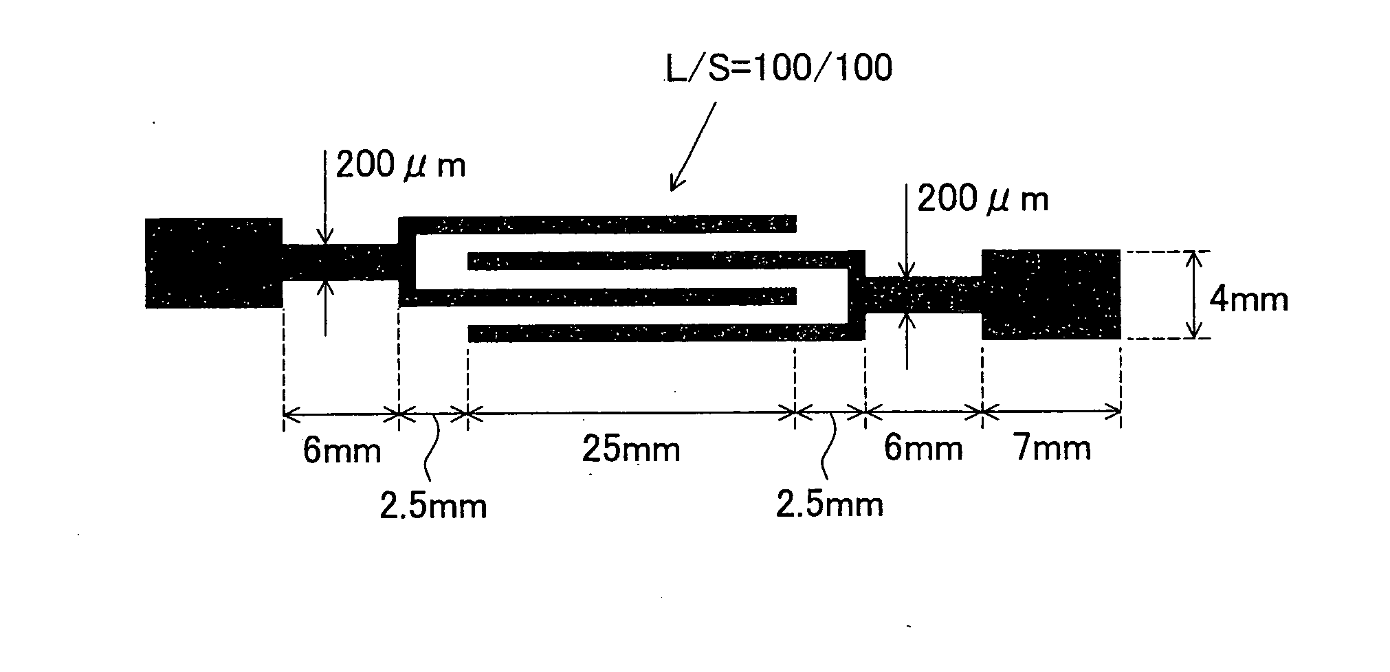
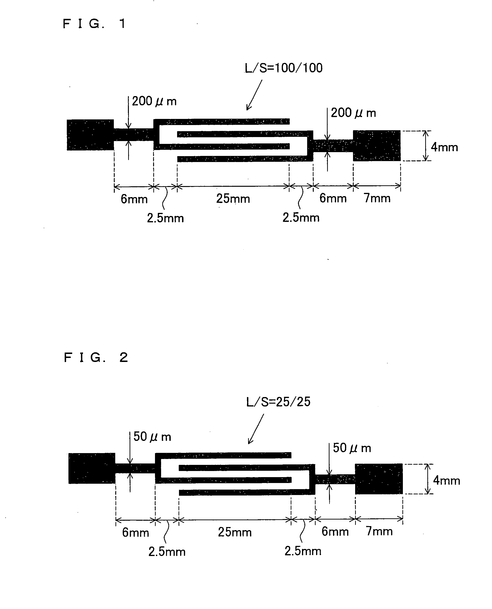
Image

Examples
synthesis example 1
Polyamide Acid
[0383]Into a 2000 ml separable flask provided with a stirring device, 29.23 g (100 mmol) of 1,3-bis(3-aminophenoxy) benzene was placed and was added to 58.46 g of dimethyl formamide in a dissolved manner, and the mixture was stirred for one hour at room temperature. Subsequently, 31.02 g (100 mmol) of 3,3′,4,4′-biphenylethertetracarboxylic acid dianhydride was added, and the mixture was stirred for three hours, thereby obtaining polyamide acid. A weight average molecular weight of polyamide acid was 100000.
synthesis example 2
Polyamide Acid
[0384]Into a 2000 ml separable flask provided with a stirring device, 31.02 g (100 mmol) of 3,3′,4,4′-biphenylethertetracarboxylic acid dianhydride and 102.7 g of dimethyl formamide were placed, and 59.68 g (40 mmol: molecular weight was 1492) of polysiloxane diamine X-22-9409S (product of Shin-Etsu Chemical Industry Co. Ltd.) was added to 59.68 g of dimethyl formamide in a dissolved manner, and the mixture was stirred at a room temperature for one hour. Subsequently, 17.54 g (60 mmol) of 1,3-bis(3-aminophenoxy)benzene was added, and the mixture was stirred for three hours, thereby obtaining polyamide acid. A weight average molecular weight of polyamide acid was 80000.
synthesis example 3
Polyamide Acid
[0385]Into a 3 L separable flask provided with a stirring device, a reflex condenser, a dropping funnel, and a tube for introducing nitrogen gas, 87.3 g (400 mmol) of pyromellitic acid dianhydride and 496 g of N-methyl pyrrolidone were placed in a nitrogen atmosphere, and an internal temperature thereof was raised to 50° C. while stirring the mixture. At this temperature, 92.6 g (100 mmol: molecular weight was 926) of polysiloxane diamine BY16-853U (product of Dow Corning Toray Silicone Co., Ltd: represented by the formula (5) where R2=propylene group, and m is about 10, a content of phenyl group was 0%) was gradually dropped from the dropping funnel for two hours. After completion of the dropping, the mixture was kept stirred for one hour at this temperature. Thereafter, a reaction temperature was lowered to 30° C. or lower, and 87.7 g (300 mmol) of 1,3-bis(3-aminophenoxy)benzene was added, and then the mixture was kept stirred for 20 hours in an nitrogen atmosphere,...
PUM
| Property | Measurement | Unit |
|---|---|---|
| thickness | aaaaa | aaaaa |
| thickness | aaaaa | aaaaa |
| thickness | aaaaa | aaaaa |
Abstract
Description
Claims
Application Information
 - R&D
- Intellectual Property
- Life Sciences
- Materials
- Tech Scout
- Unparalleled Data Quality
- Higher Quality Content
- 60% Fewer Hallucinations
Browse by: Latest US Patents, China's latest patents, Technical Efficacy Thesaurus, Application Domain, Technology Topic, Popular Technical Reports.
© 2025 PatSnap. All rights reserved.Legal|Privacy policy|Modern Slavery Act Transparency Statement|Sitemap|About US| Contact US: help@patsnap.com