

Photoelectric conversion device and solar cell using the photoelectric conversion device
a conversion device and photoelectric technology, applied in the direction of sustainable manufacturing/processing, climate sustainability, final product manufacturing, etc., can solve the problems of difficult to diffuse the alkali metal element into the photoelectric conversion layer with satisfactory stability, efficiency, and efficiency, and achieve low cost, suppress diffusion, and satisfactory stability
- Summary
- Abstract
- Description
- Claims
- Application Information
AI Technical Summary
Benefits of technology
Problems solved by technology
Method used
Image

Examples
example 1
10.1 Concrete Example 1
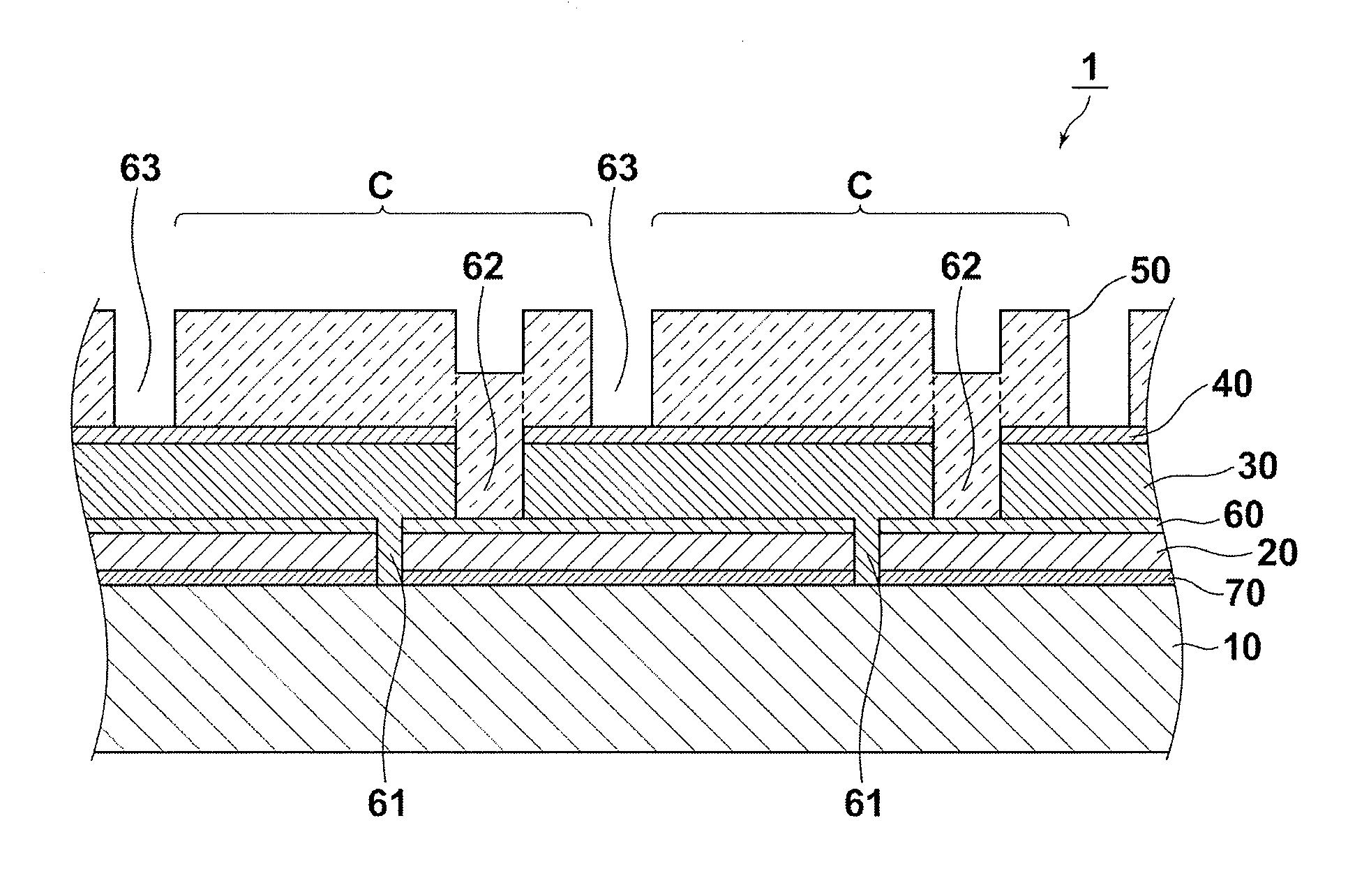
[0130]The concrete example 1 of the photoelectric conversion device according to the present invention has been produced as follows.
[0131]First, a metal substrate of the aluminum alloy 1050 (having the aluminum purity of 99.5% and the thickness of 0.30 mm) has been prepared, and an anodized film has been formed on each surface of the metal substrate by anodization under the condition that the electrolytic solution is a 0.5M water solution of oxalic acid, the electrolysis temperature is 16° C., and the DC supply voltage is 40V. Then, the metal substrate with the anodized film has been water washed and dried. Thus, an anodized substrate has been obtained, where the thickness of the anodized film has been 9.0 μm (including the thickness 0.38 μm of the barrier layer), and the diameters of the micropores have been approximately 100 nm.
[0132]Next, a film of titanium having the thickness of 50 nm has been formed as a diffusion barrier layer by evaporation on the anod...
example 2
10.3 Concrete Example 2
[0138]The concrete example 2 of the photoelectric conversion device according to the present invention has been produced in a similar manner to the concrete example 1 except that the diffusion barrier layer has been formed of chromium, instead of titanium. The photoelectric conversion efficiency of each sample of the concrete example 2 has been measured in a similar manner to the concrete example 1, and has been found to be 14% to 16%.
PUM
 Abstract
Description
Claims
Application Information