Logic Circuit and Method of Logic Circuit Design

a logic circuit and logic circuit technology, applied in the field of logic circuit design, can solve the problems of slow operation at reduced supply voltage, reduced current drive, and reduced current drive of most ptl implementations

Inactive Publication Date: 2010-09-16
TECHNION RES & DEV FOUND LTD
View PDF11 Cites 51 Cited by
  • Summary
  • Abstract
  • Description
  • Claims
  • Application Information

AI Technical Summary

Benefits of technology

[0240]The present invention successfully addresses the shortcomings of the presently known configurations by providing a fast and versatile logic circuit, with reduced area and power requirements, and capable of implementing a wide variety of logic functions and utilizing a wide variety of transistor technologies.

Problems solved by technology

Most PTL implementations, however, have two basic problems.
First, the threshold drop across the single-channel pass transistors results in reduced current drive and hence slower operation at reduced supply voltages.
Second, since the input voltage for a high logic level at the regenerative inverters is not VDD, the PMOS device in the inverter is not fully turned off, and hence direct-path static power dissipation can be significant.
The CPL technique suffers from static power consumption due to the low swing at the gates of the output inverters.
One disadvantage of DPL is the large area required by the presence of PMOS transistors.
An additional problem of existing PTL is the top-down logic design complexity, which prevents the pass-transistors from capturing a major role in real logic large-scale integration technology (LSI).
One of the main reasons for this is that no simple and universal cell library is available for PTL based design.
This creates difficulties in the development of automatic design systems for PTL logic, and in the verification of PTL logic circuit performance.
These problems are expected to appear in future high-performance technologies operating at the 10 GHz barrier, due to the increased influence of interconnect on signal delay, uncertainty in the delay of a given gate, and on-chip parameter variations.
These factors create difficulties in the design of fast digital systems controlled by a single general clock, due to considerations of delay skew between distant logic blocks, as well as the complexity of design of structures controlled by multiple clocks.
However, these desirable characteristics usually come at a cost of either silicon area, or speed, or power, and cannot be achieved all at once.
Furthermore, asynchronous circuits are typically more complicated than their synchronous counterparts.
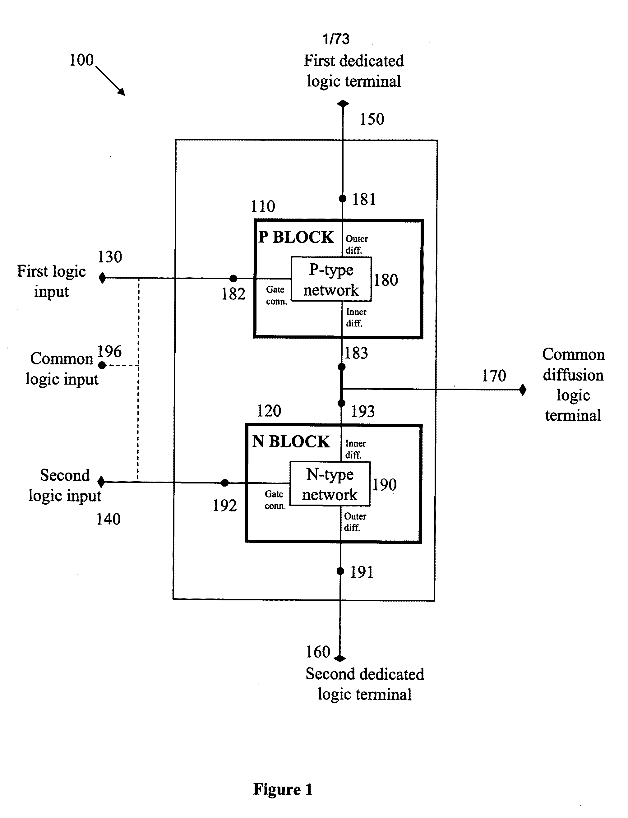
However, the generally applicability of the previously proposed GDI logic cell for logic circuit design is limited to a narrow range of CMOS technologies due to bulk effects, as discussed below.
Many GDI cell topologies cannot be implemented in standard p-well or n-well CMOS technology.
Many of the previously proposed GDI cell topologies can be implemented in standard p-well or n-well CMOS technology, due to interference of bulk effects under certain input / output conditions.
Utilizing the OR, AND and MUX implementations, in standard CMOS with VBS=0 configuration, as building blocks for more complex logic circuits is therefore problematic.
One of the common problems of PTL design methods is the low swing of output signals because of the threshold drop across the single-channel pass transistors.
The addition of a buffer stage prevents the voltage drop, but requires greater previously proposed GDI circuit area and increases circuit delay and power dissipation, making such a simplified method highly inefficient.
Interconnection effects can cause a drop in signal potential level, particularly over long interconnects.
Operation in the sub-threshold region increases delay.
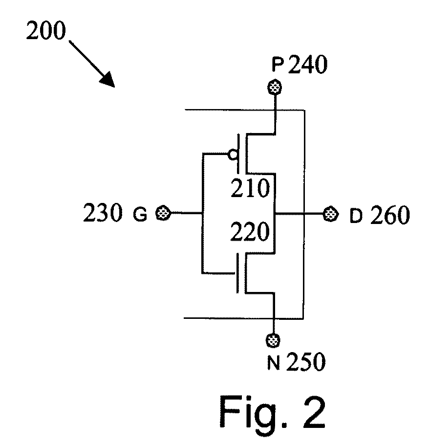
GDI logic circuits, however, have certain drawbacks, which are primarily related to input connections to MOSFET wells.
Firstly, GDI logic circuits may experience a threshold drop, and, in some cases, an increased diffusion input capacitance.
This is in contrast to PTL-based logic, which has no simple and universal cell library available.
The development of circuit synthesis tools for PTL is consequently problematic.
Using the Shannon expansion in regular logic circuits results in reduced power dissipation but requires significant area overhead.
The area overhead is caused by the additional precomputation circuitry that is required.
A similar phenomenon is partially observed in most PTL circuits, but in PTL the power consumption from the source is caused by CMOS buffers, which are included in every regular PTL.
In this sense, the PTL techniques are inferior comparatively to previously proposed GDI.
The MUX gate has the largest power consumption of all the logic gates, because of its complicated implementation (particularly in CMOS) and the presence of an additional input.
In spite of the inferior speed of previously proposed GDI relative to TG, the power-delay product of previously proposed GDI is less than both TG and CMOS.
The results of the power, delay and power-delay product of previously proposed GDI are best among the compared circuits, while N-PG has the worst performance results.
Here, as well as in the Adder circuit, the limited previously proposed GDI library was used because of process constraints.
The low frequency results represent the static power dissipation of the test chip.
The difference is caused by the fact that in all the presented circuits the simulations were performed while placing the DUT in the environment of logic circuits designed in the same technique, while in the test chip measurements the single DUT has been connected directly to output pads, causing a significantly higher load capacitance.
The results presented above show that combinational previously proposed GDI circuits are fast and low power relative to CMOS and PTL implementations.
However, due to transmission through two pass transistors, the B signal degrades by at least one VT.
The buffered previously proposed GDI C-element, however, is less area efficient.
One of the common disadvantages of pass gate logic is the static current due to VT drop, causing static power dissipation (as discussed by Al-Assadi et al.).
The previously proposed GDI circuit is slower and consumes more power than the CMOS circuit, due to the use of buffered previously proposed GDI C-elements, which are required in this case for their drive capability.
The hybrid circuit, however, consumes only half the power as CMOS while being just as fast.
The previously proposed GDI technology is not generally applicable to standard CMOS transistors.
Unnecessary constraints and complexity are thus introduced into the logic circuit design.
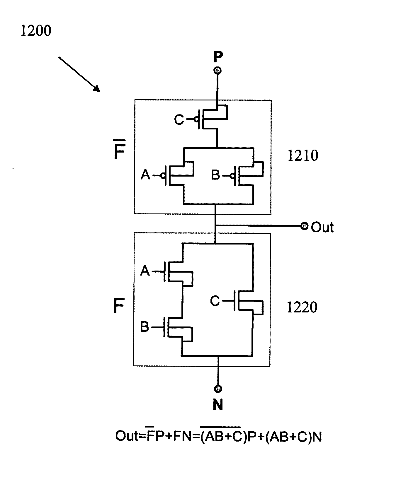
Additionally, if the F1 function is implemented in a standard n-well CMOS technology, a separate well for every PMOS transistor of each F1 cell is required, making the implementation area non-efficient.
The same problem exists when F2 is implemented in p-well CMOS technology.
In this case, a separate well for every NMOS transistor of each F2 cell is required, making the implementation non-efficient in terms of area occupation.

Method used


Image

  • Logic Circuit and Method of Logic Circuit Design
  • Logic Circuit and Method of Logic Circuit Design
  • Logic Circuit and Method of Logic Circuit Design

Examples


Embodiment Construction

[0313]The rapid development of digital applications has created a demand for faster logic circuits, having compact implementation and low power dissipation. Traditional CMOS methods, and other technologies, such as PTL, have been unable to satisfy this demand. The present invention is of a low area, power-efficient logic circuit design, referred to below as generalized gate-diffusion input (GDI+), which can be used to implement a wide variety of logic functions.

[0314]In the GDI+ cell, the bulk node of PMOS transistor is connected to the high constant voltage (referred to herein as supply voltage or VDD) and the bulk of NMOS transistor is connected to low constant voltage (referred to herein as GND). This way the proposed cell is fully compatible for implementation in a standard CMOS technology, where bulks of all PMOS transistors are connected to VDD and bulks of all NMOS transistors are connected to GND.

[0315]The GDI+ cell uses standard four-terminal NMOS and PMOS transistors and c...


PUM


Abstract

A complementary logic circuit contains a first logic input, a second logic input, a first dedicated logic terminal, a second dedicated logic terminal, a high-voltage terminal configured for connection to a high constant voltage a low-voltage terminal configured for connection to a low constant voltage, a p-type transistor, and an n-type transistor. The p-type transistor has an outer diffusion connection, a gate connection, an inner diffusion connection, and a bulk connection. The n-type transistor has an outer diffusion connection, a gate connection, an inner diffusion connection, and a bulk connection. The first dedicated logic terminal is connected to the outer diffusion connection of the p-type transistor, the second dedicated logic terminal is connected to the outer diffusion connection of the n-type transistor, the inner diffusion connection of the p-type transistor and the inner diffusion connection of the n-type transistor is connected to form a common diffusion logic terminal, the high-voltage terminal is connected to the bulk connection of the p-type transistor, and the low-voltage terminal is connected to the bulk connection of the n-type transistor.

Description

FIELD AND BACKGROUND OF THE INVENTION[0001]The present invention relates to a logic circuit design and, more particularly, to a logic circuit design for combinatorial and asynchronous logic circuits.[0002]A large body of research has been performed to develop and improve traditional Complementary Metal Oxide Semiconductor (CMOS) techniques for the production of integrated circuits (ICs). The object of this research is to develop a faster, lower power, and reduced area alternative to standard CMOS logic circuits (see A. P. Chandrakasan, S. Sheng, R. W. Brodersen, “Low-Power CMOS Digital Design”, IEEE Journal of Solid-State Circuits, vol. 27, no. 4, pp. 473-484, April 1992, and in A. P. Chandrakasan, R. W. Brodersen, “Minimizing Power Consumption in Digital CMOS Circuits”, Proceedings of the IEEE, vol. 83, no. 4, pp. 498-523, April 1995.) This research has resulted in the development of many logic design techniques during the last two decades. One popular alternative to CMOS is pass-t...

Claims


Application Information

Patent Timeline
Patent Type & Authority Applications(United States)
IPC IPC(8): H03K19/0948G06F17/50
CPCH03K19/0948
Inventor FISH, ALEXANDERMORGENSHTEIN, ARKADIY
Owner TECHNION RES & DEV FOUND LTD
Why Eureka
Try Eureka