
Field effect transistor

a field effect transistor and transistor technology, applied in the field of field effect transistors, can solve the problems of high breakdown voltage, high difficulty in selectively forming a high-concentration psup>+/sup>-type layer by a method such as ion implantation, and the need for a higher breakdown voltage, so as to facilitate normal operation and achieve high breakdown voltage. , the effect of large current operation

Active Publication Date: 2010-09-30
FURUKAWA ELECTRIC CO LTD
View PDF6 Cites 15 Cited by
  • Summary
  • Abstract
  • Description
  • Claims
  • Application Information

AI Technical Summary

Benefits of technology

[0019]It is an object of the present invention to at least partially solve the problems in the conventional technology. In order to solve the problems described above, the present invention is a field effect transistor that uses a III-nitride semiconductor with a body electrode being formed on either the top surface or the bottom surface of that III-nitride semiconductor. In so doing, it is possible to easily realize normally-off operation. With the present invention, it is possible to provide a field effect transistor that is capable of normally-off operation, high breakdown voltage and large current operation.

Problems solved by technology

Generally, normally-off operation is difficult for an AlGaN based HFET, however, by forming a gate electrode in a recess that is formed by removing a part of the carrier induction layer and a part of the barrier layer so that the film thickness of the barrier layer is equal to or less than the critical thickness, normally-off operation is made possible, and by controlling the film thickness of the barrier layer at the atomic layer level, it is possible to keep fluctuation in the threshold voltage small.
However, in the case of GaN, selectively forming a high-concentration p+-type layer by a method such as ion implantation method is extremely difficult.
The GaN based MOSFET of non-patent document 1 has a breakdown voltage of 940 V; however, for use in a power-supply circuit of an automobile, there is a problem in that even higher breakdown voltage is necessary.
Furthermore, in order to realize a GaN based power device by using a method in which an electrode is disposed in a p+-type layer and holes are removed as in an Si power device, it is necessary to form a p+-type layer having a sheet carrier density of 1×1015 cm−2 at least, however, there is a problem in that a sheet carrier density of 7×1012 cm−2 of a p+-type layer that can be formed in GaN as given in non-patent document 3 is too low.
Also, it is even more difficult to selectively form a high-concentration p+-type layer.

Method used


Image

  • Field effect transistor
  • Field effect transistor
  • Field effect transistor

Examples


first embodiment

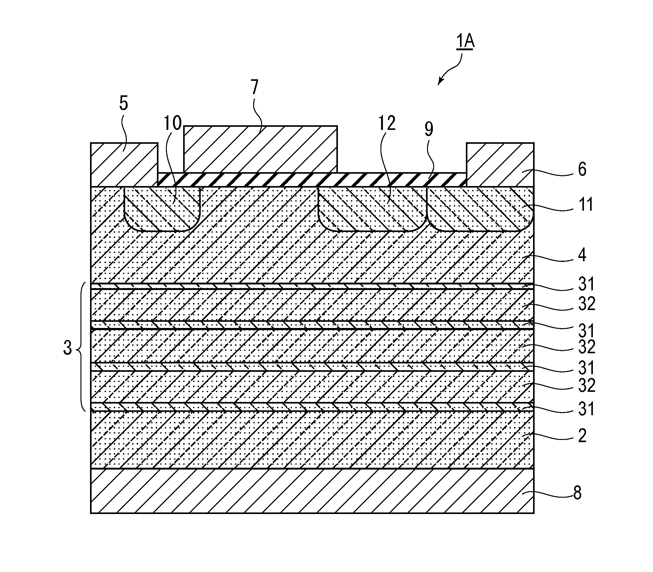
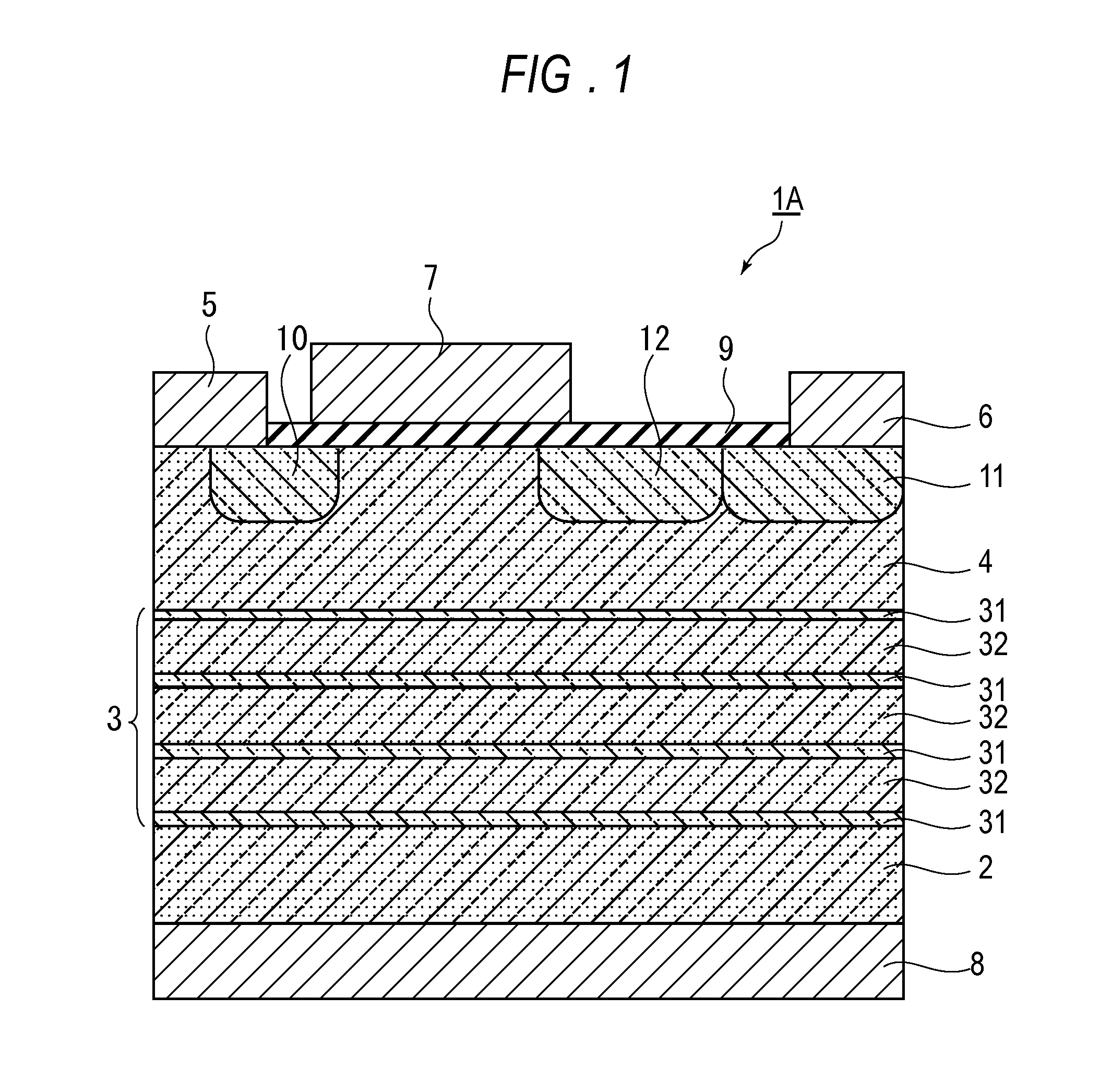
[0026]FIG. 1 is a cross-sectional drawing showing the construction of a field effect transistor 1A that uses a III-nitride (GaN) of a first embodiment of the present invention. In this embodiment GaN and AlN are used as the III-nitride.

[0027]This field effect transistor 1A comprises a p-type Si substrate 2 as the substrate, on which a semiconductor layer comprising a p-type GaN layer 4 is formed via a buffer layer 3. A body electrode 8 is provided on the bottom surface of the p-type Si substrate 2.

[0028]Moreover, n+-type GaN layers 10, 11, which are contact layers, are formed in regions on the surface of the p-type GaN layer 4 that come in contact with the bottom of a source electrode 5 and drain electrode 6. There is also a RESURF layer 12 for reducing the electric field concentration provided in a region on the surface of the p-type GaN layer 4 that is underneath the section between a gate electrode 7 and drain electrode 6. Furthermore, a SiO2 layer 9, which is a gate oxidation fi...

second embodiment

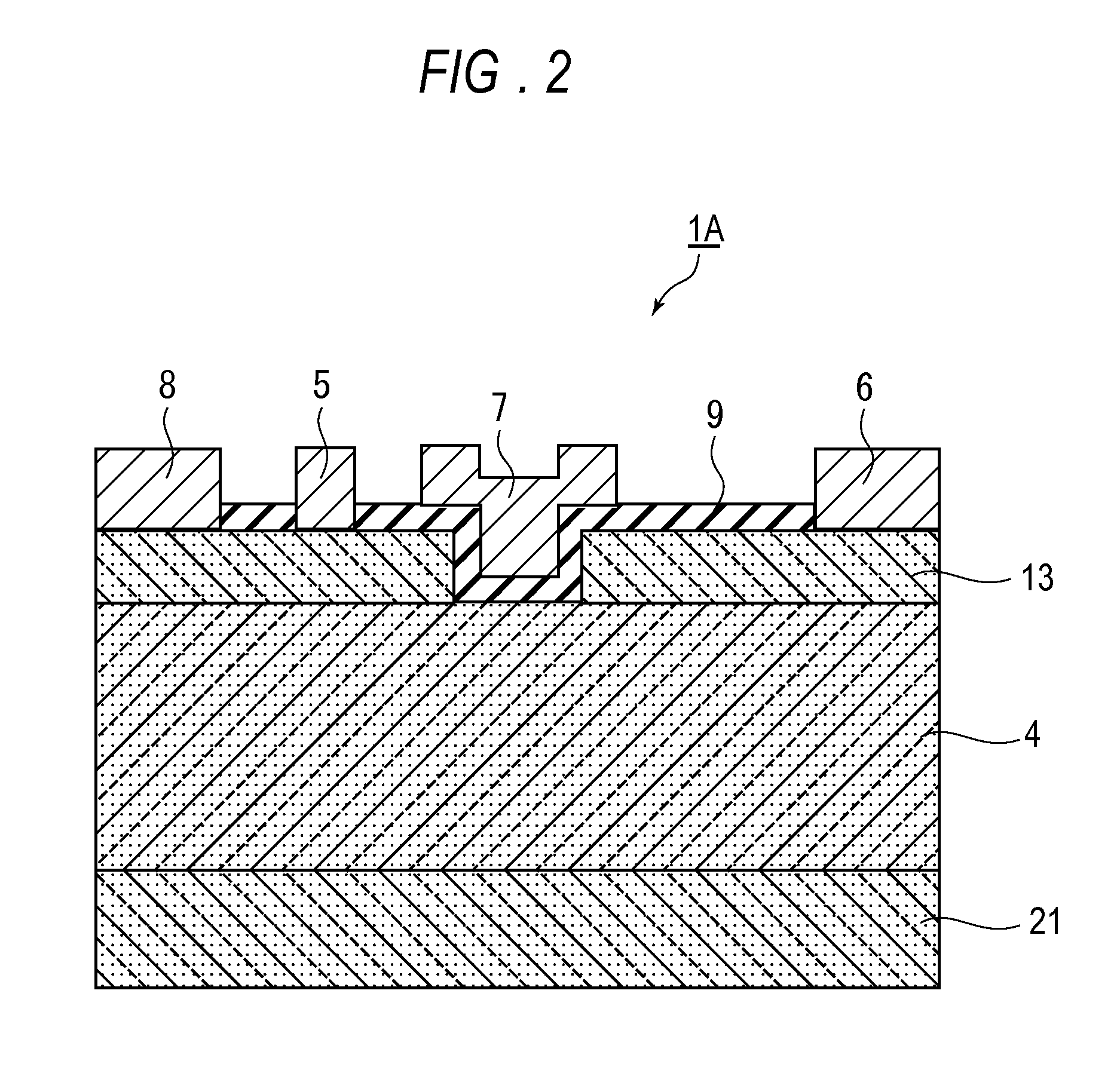
[0056]FIG. 2 is a cross-sectional drawing showing the structure of a field effect transistor 1B of a second embodiment of the present invention. In the case of the III-nitride semiconductor field effect transistor 1B, the body electrode 8 is formed on the top surface of the III nitride semiconductor field effect transistor 1B.

[0057]As shown in FIG. 2, the III nitride semiconductor field effect transistor 1B uses a sapphire substrate 21, with a p-type GaN layer 4 being formed on the sapphire substrate 21. Furthermore, an AlGaN layer 13 is formed on a top surface of the p-type GaN layer 4 underneath a source electrode 5, drain electrode 6 and body electrode 8. Here, the film thickness of this AlGaN layer 13 is approximately 20 nm. The band gap energy of AlGaN is larger than that of GaN, however, the film thickness is thin, so electrons from a metal electrode permeate to the p-type GaN layer 4 due to the tunnel effect, and it is possible to keep the resistance at the boundary between t...

example

[0076]Test results of the breakdown voltage are explained below using an example of the III-nitride (GaN) field effect electrode of the second embodiment of the present invention and a comparative example.

(Crystal Growth Step)

[0077]With the substrate temperature of the sapphire substrate 21 at 1000° C., a 1-μm-thick p-type GaN layer 4 was grown on the sapphire substrate 21 by the MOCVD method, after which the substrate temperature was raised to 1050° C. and a 2-μm-thick Mg doped GaN layer was formed. Mg was used as the p-type dopant, and the Mg concentration was 1×1017 cm−3. Next, a 25-nm-thick AlGaN layer (Al composition 25%) was grown to form the AlGaN layer 13.

(Device Isolation Step)

[0078]Next, photoresist was applied to the surface of the AlGaN layer 13, and patterning for device isolation was performed by exposure and developing processes, after which a dry etching apparatus was used to etch the AlGaN layer 13 and Mg doped p-type GaN layer 4 to a depth of 200 nm. The photoresis...


PUM


Abstract

Provided is a GaN based field effect transistor that is capable of normally-off operation, high breakdown voltage and large current. A body electrode 8 is provided on the bottom surface or the top surface of the field effect transistor. When the body electrode 8 is provided on the bottom surface, a p-type GaN layer 4 is provided on a p-type Si substrate 2 via a buffer layer 3 comprising a plurality of AlN layers 31 and GaN layers 32, with the top layer of that buffer layer 3 being a thin AlN layer 31, and the body electrode 8 being formed on the bottom surface of the p-type Si substrate. When the body electrode 8 is provided on the top surface, a p-type GaN layer 4 is provided on a sapphire substrate 21 and an AlGaN layer 13 is provided on the area under the source electrode 5 and drain electrode 6, with the body electrode 8 being provided on top of the AlGaN layer 13. Holes 20 that are generated by an avalanche phenomenon run through the body electrode 8.

Description

CROSS-REFERENCE TO RELATED APPLICATIONS[0001]This application claims priority from Japanese patent application serial No. 2009-076047, filed on Mar. 26, 2009, the entire content of which is incorporated herein by reference.BACKGROUND OF THE INVENTION[0002]1. Field of the Invention[0003]The present invention relates to a field effect transistor that uses a III-nitride semiconductor, and more particularly to a field effect transistor that realizes normally-off operation, and has high breakdown voltage and large current operation.[0004]2. Description of the Related Art[0005]Due to the intrinsic properties of the material, III-nitride semiconductors such as GaN have higher breakdown voltage and larger current density than that of silicon semiconductors, and are capable of high-temperature operation, which makes them being expected as power devices.[0006]GaN based MOSFETs (Metal Oxide Semiconductor Field Effect Transistors) (refer to non-patent document 1) and AlGaN / GaN based HFETs (Hete...

Claims


Application Information

Patent Timeline
Patent Type & Authority Applications(United States)
IPC IPC(8): H01L29/772H01L29/06
CPCH01L21/02381H01L21/02458H01L21/02507H01L29/78H01L29/2003H01L29/66522H01L29/778H01L21/0254
Inventor NIIYAMA, YUKINOMURA, TAKEHIKOKATO, SADAHIRO
Owner FURUKAWA ELECTRIC CO LTD
Learn More