Lithographic systems and methods with extended depth of focus

a lithographic system and depth of focus technology, applied in the direction of microlithography exposure apparatus, printers, instruments, etc., can solve the problems of increasing complexity and cost, adding approximately one-third to the overall cost, and adding a large cost to the finished semiconductor component of optical lithography, so as to reduce unwanted effects and increase the depth of focus

Active Publication Date: 2010-10-14
OMNIVISION TECH INC
View PDF2 Cites 3 Cited by
  • Summary
  • Abstract
  • Description
  • Claims
  • Application Information

AI Technical Summary

Benefits of technology

[0014]Systems and methods are provided to increase depth of focus and control focus related aberrations within optical lithography, as compared to the prior art. In certain embodiments herein, such systems and methods further reduce unwanted effects within optical lithography relating to (a) misfocus, (b) misalignment of the semiconductor component and / or mask, (c) thermal changes, and / or (d) optical aberrations such as field curvature (which limits the region of good focus).
[0015]Systems and methods are provided that maintain a desired shape of features in the aerial image above the threshold of the lithographic recording medium (e.g., photoresist) over a large range of misfocus, thereby preserving the resolution of the system even with relaxed tolerances of assembly and use. In some cases, the shape of a desired aerial image above a threshold is maintained. In other cases, the numerical aperture (NA) of the system can be increased without reducing the depth of focus. In other cases, the system response of the imaging system can be tailored to match the spatial frequency content of the desired aerial image. In still other cases, the NA of a lens design can be increased to a higher value than in the original design, thereby increasing the resolution without the loss in depth of focus that would normally occur.
[0021]In another embodiment, a method increases the process window for lithography by: illuminating a reticle and imaging a wavefront of the reticle to an aerial image by altering phase of the wavefront such that aerial image has extended depth of focus and an increased process window size as compared to an aerial image formed without altering of the wavefront phase.

Problems solved by technology

Optical lithography nonetheless adds large cost to a finished semiconductor component, adding approximately one-third to the overall cost.
As the operating wavelength decreases to 193 nm to produce reduced feature size, for example at 90 nm, the exposure source and optical components of the lithographic system also increase in complexity and cost.
As the complexity of ICs increases, requirements to produce ever smaller features on the components (and hence in the patterns) are generated.
An increase in resolution is therefore not useful without adequate DOF.
The reduced DOF raises other issues that include, for example, wafer flatness, wafer warping, thickness of the photo-resist, and reticle flatness.
For example, even though the tolerance on the reticle flatness is reduced by the square of any demagnification, the decrease in DOF requires flatter reticles, thereby increasing the cost of ‘mask blank’ (reticles prior to patterning) manufacture.
Also, stress from chromium deposition during the patterning of the mask blank may also cause it to warp.
Problems may also occur during use of a reticle when the deposited chromium absorbs radiation, increasing its temperature and causing irregular thermal expansion.
Periodic reticle realignment is frequently required, reducing productivity of the optical lithographic system.
Non-correctable registration errors become significant for the 100 nm node and beyond.
Thus DOF and focus related aberrations, e.g., field curvature, become major limitations of optical lithography.
Since the 1980s, optical lithography has attempted to employ phase shift masks to improve this problems associated with DOF; however such efforts have not been successful due to increased complexity of the exposure source and optics within the lithographic system.
To date, therefore, the prior art efforts to extend the depth of focus have been limited to 15% improvement.

Method used


Image

  • Lithographic systems and methods with extended depth of focus
  • Lithographic systems and methods with extended depth of focus
  • Lithographic systems and methods with extended depth of focus

Examples


Embodiment Construction

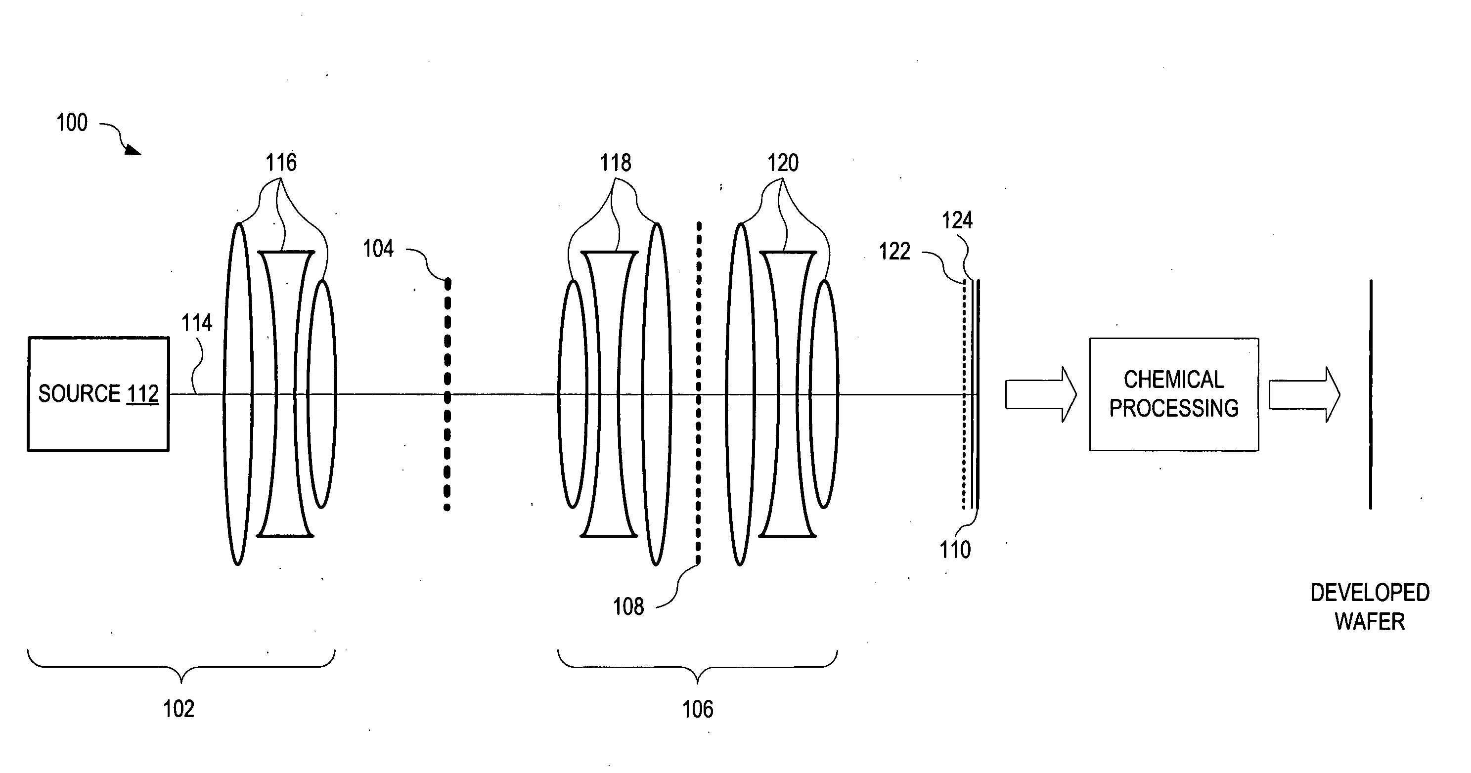
[0060]FIG. 1 illustrates an optical lithographic system 100 for extending depth of focus (DOF). System 100 is shown with an illumination system 102, a reticle 104, an imaging lens 106 that implements wavefront coding through a pupil plane function 108, and a wafer 110. Illumination system 102 is shown with an optical radiation source 112 and a lens group 116. Source 112 generates optical radiation 114 that passes through lens group 116, reticle 104 and imaging lens 106, including includes pupil plane function 108, to produce an aerial image 122. Reticle 104 is constructed such that a desired pattern is formed in aerial image 122, as described in more detail below. Imaging lens 106 may include lens groups 118 and 120, as shown. Imaging lens 106 operates to image reticle 104, illuminated by radiation 114, to produce aerial image 122. In one embodiment, radiation 114 is selected from the ultraviolet spectrum.

[0061]Lens groups 116, 118 and 120 may, for example, include (a) one or more o...


PUM

PropertyMeasurementUnit
wavelengthsaaaaaaaaaa
wavelengthaaaaaaaaaa
illumination wavelengthaaaaaaaaaa

Abstract

An optical lithography system that has extended depth of focus exposes a photoresist coating on a wafer, and includes an illumination sub-system, a reticle, and an imaging lens that has a pupil plane function to form an aerial image of the reticle proximate to the photoresist. The pupil plane function provides the extended depth of focus such that the system may be manufactured or used with relaxed tolerance, reduced cost and / or increased throughput. The system may be used to form precise vias within integrated circuits even in the presence of misfocus or misalignment.

Description

RELATED APPLICATIONS[0001]This application is a divisional application of U.S. patent application Ser. No. 10 / 858,337, filed Jun. 1, 2004, which claims priority to U.S. Provisional Application Ser. No. 60 / 474,318, filed May 30, 2003, which is incorporated herein by reference.U.S. GOVERNMENT RIGHTS[0002]This invention was made with Government support under DAAH01-03-C-R202 awarded by the U.S. Army Aviation and Missile Command. The Government has certain rights in the invention.BACKGROUND[0003]Semiconductor manufacturing of devices such as integrated circuits relies upon lithography to replicate a pattern onto components (e.g., wafers, substrates, microchips). A traditional optical lithographic system includes an exposure source, illumination optics, an object mask or reticle, photoresist and process methodology to transfer the pattern from a mask or reticle, to photoresist, and to the components. Although several types of lithography exist, optical lithography remains favored because...

Claims


Application Information

Patent Timeline
Patent Type & Authority Applications(United States)
IPC IPC(8): G03B27/52G02B27/00G03B27/00G03F7/20
CPCG02B27/0025G03F1/144G03F7/705G03F7/70125G03F7/70308G03F1/36
Inventor DOWSKI, JR., EDWARD RAYMONDJOHNSON, GREGORY E.KUBALA, KENNETH S.CATHEY, JR., WADE THOMAS
Owner OMNIVISION TECH INC
Why Eureka
Try Eureka