
Substrate having single patterned metal layer, and package applied with the substrate , and methods of manufacturing of the substrate and package

a technology of metal layer and substrate, applied in the direction of resistive material coating, printed circuit non-printed electric components association, nuclear engineering, etc., can solve the problems of increasing the complexity of the plating process for filling the through hole, the requirement of systematic integration of downstream products, and the difficulty of achieving high-efficiency wiring on bga substrates or lead frame substrates. achieve the effect of reducing the thickness of the substrate, high production yield and thin profil

Active Publication Date: 2010-11-18
ADVANCED SEMICON ENG INC
View PDF55 Cites 56 Cited by
  • Summary
  • Abstract
  • Description
  • Claims
  • Application Information

AI Technical Summary

Benefits of technology

[0012]The present invention provides structures of the substrate having a single patterned metal layer, and the package with this substrate, and methods of manufacturing the same. The substrate of the disclosure merely includes a patterned metal layer (as conductive traces) and a patterned base, which reduces the thickness of the substrate. This extra thin substrate is particularly suitable for the application of small-sized, low profile products. Also, the simplified process for manufacturing the substrate is suitable for mass production, while high production yield is still maintained. Compared to the prior art, the substrate structure of the disclosure satisfies the desired requirements of the electronic product with thin profile and low cost.

Problems solved by technology

Thus, it is very difficult to achieve a high efficiency wiring on a BGA substrate or a lead frame substrate.
Besides, in addition to the request of the flip chip technology, the request of systematic integration of the downstream products is also getting more and more urgent.
However, plating procedure for filling the through hole requires more complicated technique and longer time to plate.
However, it is difficult to further reduce the size of the conventional structures (such as substrates of FIG. 1F and FIG. 2) using the known manufacturing methods.
Besides the size and electrical properties, manufacturing cost of the substrate is also a considerable factor in the device application, especially for the small device with lower market price.

Method used


Image

  • Substrate having single patterned metal layer, and package applied with the substrate , and methods of manufacturing of the substrate and package
  • Substrate having single patterned metal layer, and package applied with the substrate , and methods of manufacturing of the substrate and package
  • Substrate having single patterned metal layer, and package applied with the substrate , and methods of manufacturing of the substrate and package

Examples


first embodiment

[0036]FIG. 3A˜FIG. 3F schematically shows a progressive flow of manufacturing a substrate having single patterned metal layer according to the first embodiment of the present invention.

[0037]First, a base 201 is provided, and a metal layer 202 is formed on the base 201, as shown in FIG. 3A. The metal layer 202 includes an upper surface 202a and a lower surface 202b.

[0038]The base 201 can be formed of a variety of materials, such as resin or dielectric materials. Examples of resin materials of the base 201 include Ajinomoto build-up film (ABF), bismaleimide triazine (BT), polyimide (PI), liquid crystal polymer (LCP), epoxy, resin with a single copper foil, prepreg (PP), and other resin materials. The resins may be reinforced with glass fibers which can be woven or fiber mat or filled with a particulate filler. Alternatively, the base 201 may be formed of solder mask (SM), liquid crystal polymer (LCP), prepreg (PP), or other dielectric materials. It is not intended that the material ...

second embodiment

[0054]Besides substrates S1 and S2 of the first embodiment, the substrate structure can be varied by slightly modifying the methods described above without departing from the spirit of the invention. The features of the second embodiment identical to the features of the first embodiment are designated with the same reference numbers.

[0055]FIG. 6A˜FIG. 6F schematically shows a progressive flow of manufacturing a substrate having a single patterned metal layer according to the second embodiment of the present invention. The processes of manufacturing the substrates of the first and second embodiments are similar except for a change in the formation the patterned metal layer and the first surface finish layer. Same features in the drawings of the first and second embodiments are designated with the same reference numbers, and redundant discussion is omitted.

[0056]First, a base 201 is provided, and a metal layer 202 is formed on the base 201, as shown in FIG. 6A. The metal layer 202 inc...

third embodiment

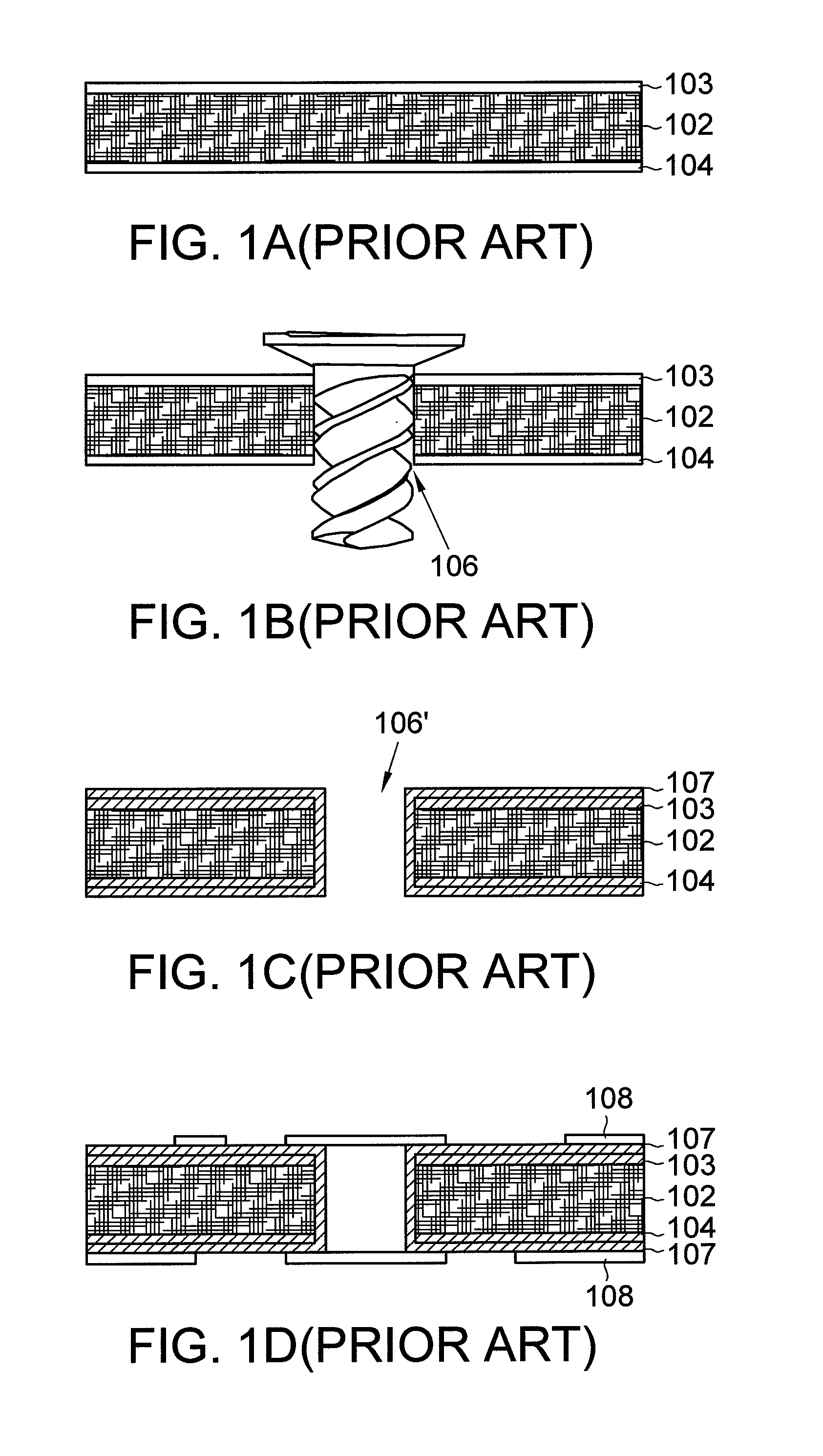
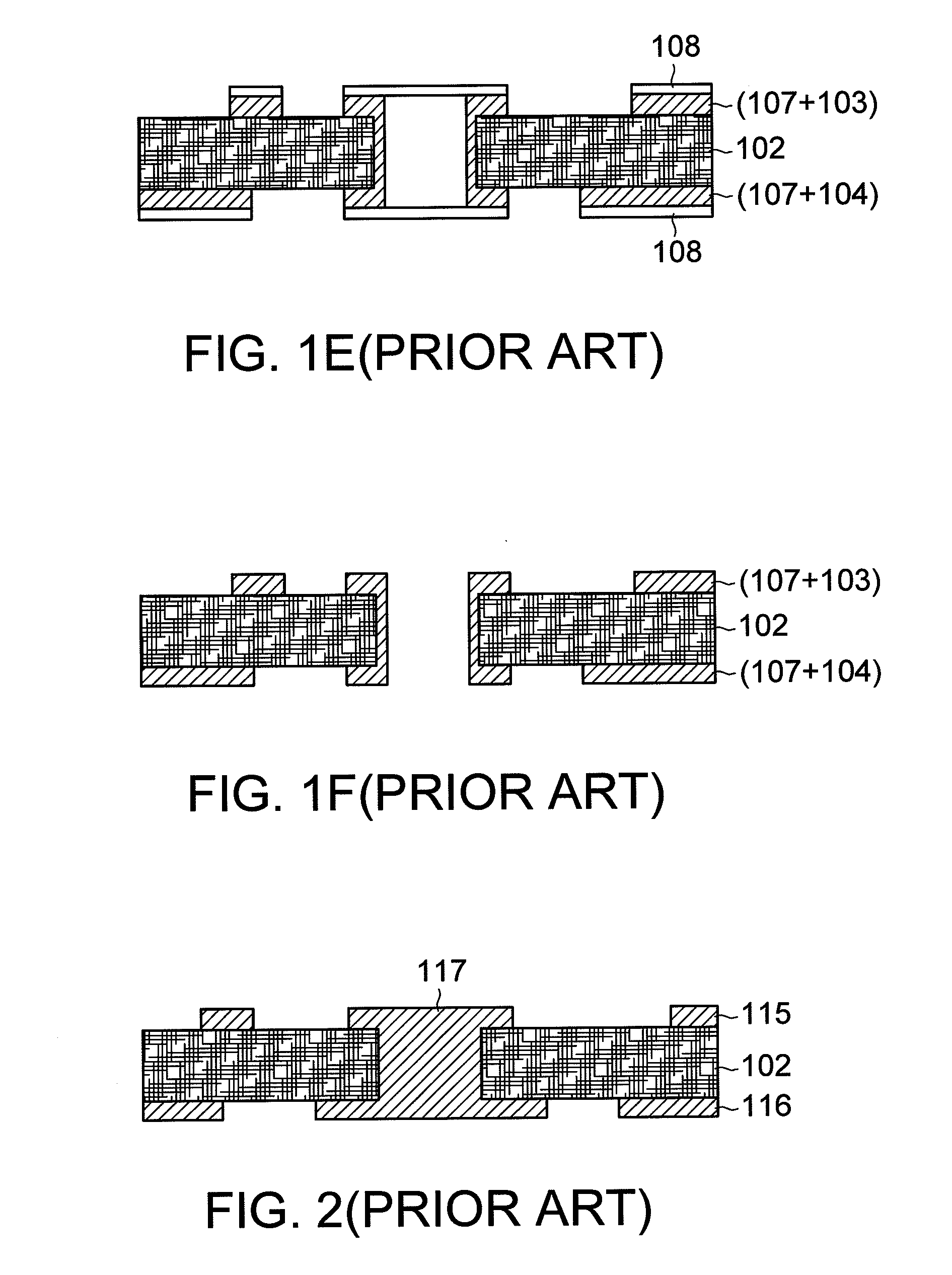
[0070]The methods disclosed in the first and second embodiments adopt the substrates with the base 201 formed of resin material. In the third embodiment, the base 201 formed of dielectric material is exemplified for describing the progressive flow of manufacturing the substrate. Also, a carrier is adopted in the third embodiment during substrate fabrication.

[0071]FIG. 8A˜FIG. 8F schematically shows a progressive flow of manufacturing a substrate having a single patterned metal layer according to the third embodiment of the present invention.

[0072]First, a carrier 20 is provided. A metal layer 401 is formed on the carrier 20, and a base 402 is formed on the metal layer 401, as shown in FIG. 8A. The base 402 may be formed of solder mask (SM), liquid crystal polymer (LCP), prepreg (PP), or other dielectric materials.

[0073]Next, the base 402 is patterned to form a patterned base 402′ with a plurality of apertures 402a and through holes 402b, as shown in FIG. 8B. The patterning of the ba...


PUM

PropertyMeasurementUnit
thicknessaaaaaaaaaa
surface finishaaaaaaaaaa
conductiveaaaaaaaaaa

Abstract

A substrate having single patterned metal layer includes a patterned base having at least a plurality of apertures, the patterned metal layer disposed on the patterned base, and a first surface finish layer. Parts of the lower surface of the patterned metal layer are exposed by the apertures of the patterned base to form a plurality of first contact pads for downward electrical connection externally, and parts of the upper surface of the patterned metal layer function as a plurality of second contact pads for upward electrical connection externally. The first surface finish layer is disposed at least on one or more surfaces of the second contact pads, and the first surface finish layer is wider than the second contact pad beneath. A package applied with the substrate disclosed herein further comprises at least a die conductively connected to the second contact pads of the substrate.

Description

[0001]This application claims the benefit of U.S. Provisional Application No. 61 / 177,652, filed May 13, 2009, the subject matter of which is incorporated herein by reference.BACKGROUND OF THE INVENTION[0002]1. Field of the Invention[0003]The invention relates in general to a substrate and a package and methods of manufacturing the same, and more particularly to the substrate having a single patterned metal layer, and a package applying the substrate, and methods of manufacturing the substrate and the package.[0004]2. Description of the Related Art[0005]The integrated circuit (IC) package technology plays an important role in the electronics industry. Electronic packaging is for protecting and supporting circuit configuration, creating a path for heat dissipation and providing modularized standard specification form factors for the parts. Electronic packaging in 1990s mainly employs ball grid array (BGA) packaging which is excellent in heat dissipation, has excellent electrical prope...

Claims


Application Information

Patent Timeline
Patent Type & Authority Applications(United States)
IPC IPC(8): H05K1/18H05K1/03H05K1/02B05D5/12B05D3/06
CPCH01L21/486H01L21/6835H01L23/3121H01L23/498H01L23/49827H01L24/12H01L24/16H01L24/28H01L24/32H01L24/45H01L24/48H01L2221/68345H01L2224/13099H01L2224/13144H01L2224/13147H01L2224/16225H01L2224/2919H01L2224/32057H01L2224/32225H01L2224/45124H01L2224/45139H01L2224/45144H01L2224/45147H01L2224/48091H01L2224/48227H01L2224/484H01L2224/48599H01L2224/48699H01L2224/73265H01L2224/83385H01L2924/01013H01L2924/01027H01L2924/01028H01L2924/01029H01L2924/01033H01L2924/01046H01L2924/01047H01L2924/0105H01L2924/01059H01L2924/01075H01L2924/01078H01L2924/01079H01L2924/01082H01L2924/014H01L2924/14H01L2924/01005H01L2924/01006H01L2924/01074H01L2924/0132H01L2924/157H01L2224/29111H01L2924/00014H01L2924/0665H01L2924/00012H01L2924/00H01L24/73H01L2224/85439H01L2224/85444H01L2224/85455H01L2224/85664H01L2924/181H01L2224/45015H01L2924/207
Inventor APPELT, BERND KARLCHEN, WILLIAM T.CHEUNG, CALVINHUANG, SHIH-FUSU, YUAN-CHANGCHEN, CHIA-CHENGLEE, TA-CHUN
Owner ADVANCED SEMICON ENG INC
Features
  • Generate Ideas
  • Intellectual Property
  • Life Sciences
  • Materials
  • Tech Scout
  • Unparalleled Data Quality
  • Higher Quality Content
  • 60% Fewer Hallucinations
Learn More