Diamond semiconductor device

Inactive Publication Date: 2010-11-18
NAT INST FOR MATERIALS SCI
View PDF1 Cites 10 Cited by
  • Summary
  • Abstract
  • Description
  • Claims
  • Application Information

AI Technical Summary

Benefits of technology

[0005]An object of the present invention is to provide a diamond semiconductor device being able to extract the function of the hydrogen termination thereof to the utmost extent whereas preventing

Problems solved by technology

However, in the conventional semiconductor devices, a hydrogen termination is formed also on the substrate surface where electrodes are not fabricated, leading to not only an electric conduction from the electrode to the diamond bulk via the diamond interface, but also electric conduction in the substrate surface between the electrodes, or

Method used


Image

  • Diamond semiconductor device
  • Diamond semiconductor device
  • Diamond semiconductor device

Examples


example 1

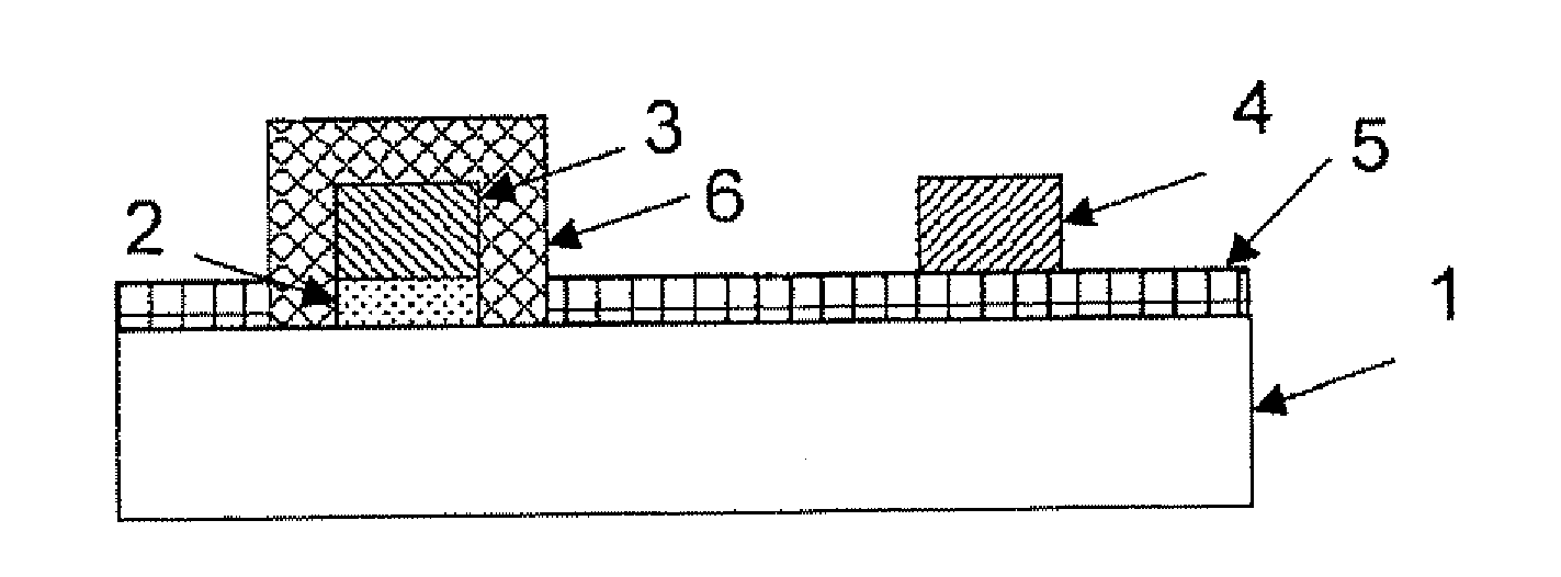
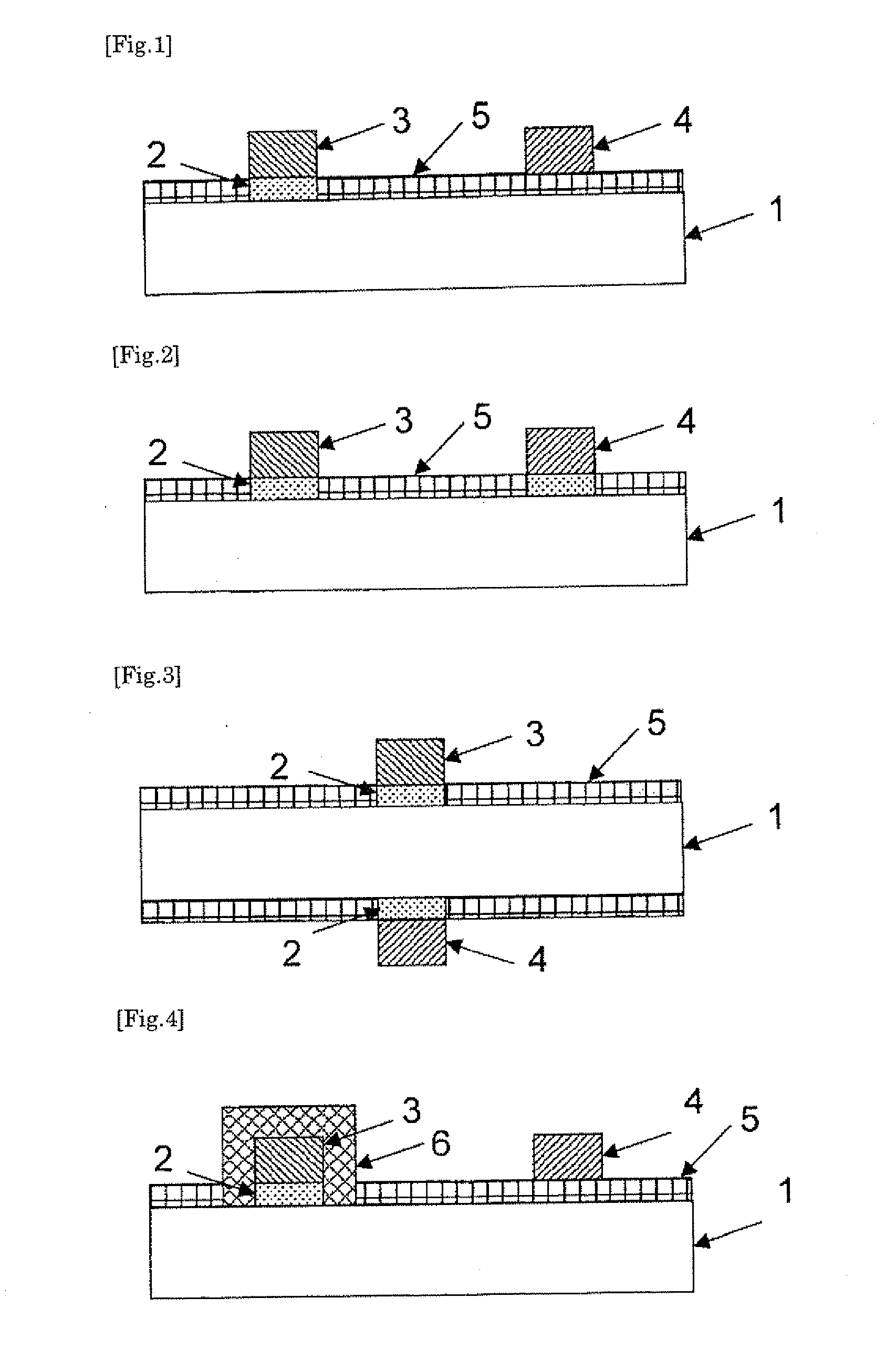
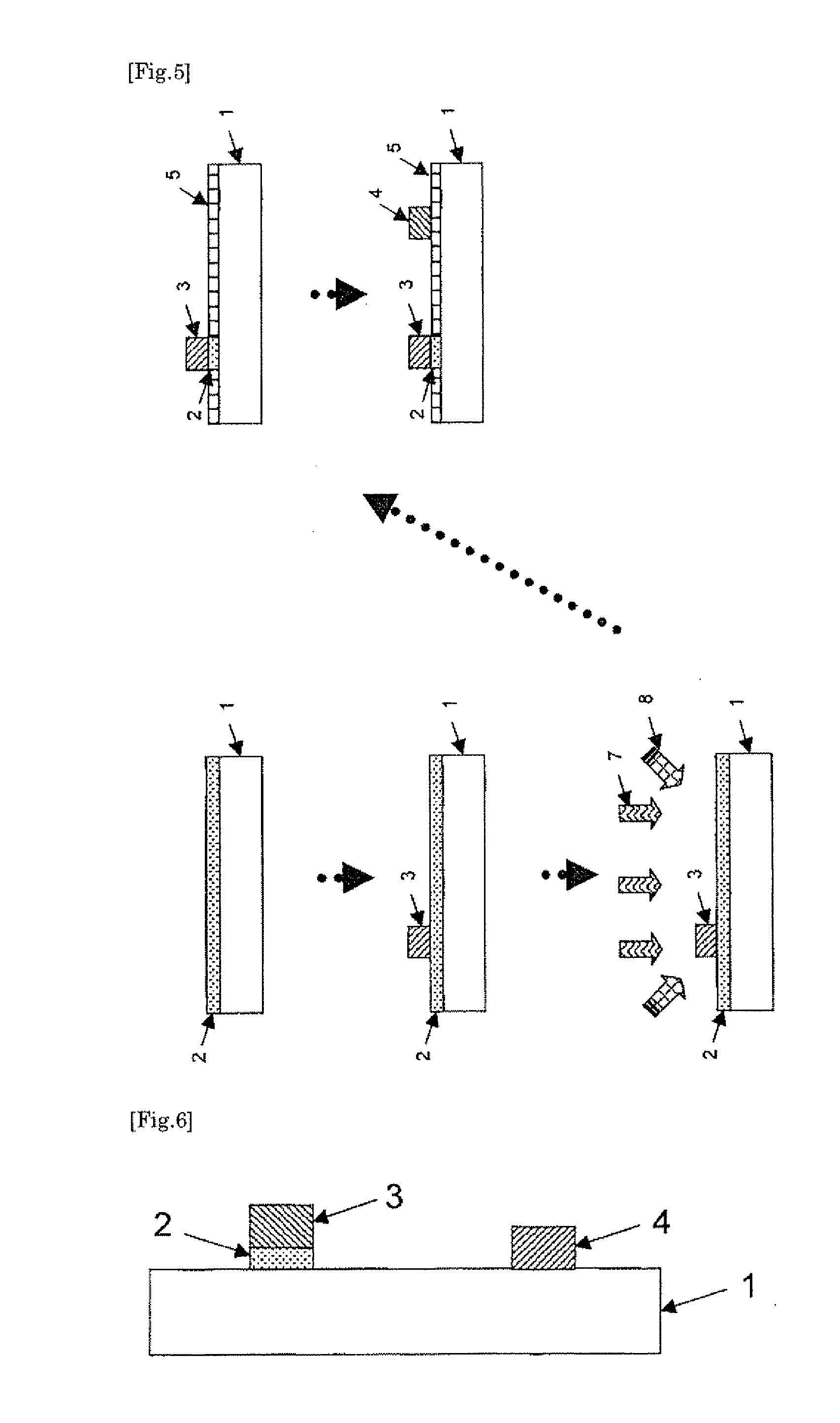
[0086]A p-type semiconducting single crystal doped with boron at a concentration of 2×1015 cm−3 (dimension: 3 mm length×3 mm width×20 μm thickness) was formed on a high-resistance diamond single crystal (dimension: 3 mm length×3 mm width×0.5 mm thickness), and the thus-formed crystal was used as a substrate. In the same manner as in the above-mentioned Reference Example, the surface of the single-crystal substrate (1) was processed for hydrogen termination.

[0087]Next, using gold as an electrode material, an electrode (3) having a thickness of 40 nm was formed on the hydrogen-terminated surface (2), according to a vacuum vapor deposition method.

[0088]Next, using an excimer lamp, UV rays at a wavelength of 172 nm were radiated to the substrate (1) with the electrode (3) formed thereon, at an irradiance of 10 mW / cm2 for an irradiation time of 10 minutes in an oxygen atmosphere under the condition of an oxygen partial pressure of 100 Torr, thereby forming an insulating region by oxygen ...

example 2

[0091]A diamond semiconductor device having the structure shown in FIG. 2 was fabricated in the same manner as in Example 1, in which, however, the electrode (4) of gold was formed on the hydrogen-terminated surface (2).

[0092]The diamond semiconductor device was tested for the electric conductivity characteristics thereof at room temperature according to a current-voltage test method in the same manner as in Example 1. The test result is shown in FIG. 13 as a graph. The graph confirms good conductivity. No surface leakage current was detected.

example 3

[0093]A p-type semiconducting single crystal doped with boron at a concentration of 1×1016 cm−3 (dimension: 3 mm length×3 mm width×0.5 mm thickness) was used as a substrate; and in the same manner as in the above-mentioned Reference Example, both surfaces of the single-crystal substrate (1) were processed for hydrogen termination.

[0094]Next, using gold as an electrode material, an electrode (3) having a thickness of 40 nm was formed on the hydrogen-terminated surface (2), according to a vacuum vapor deposition method; and then similarly, using gold as an electrode material, an electrode (4) having a thickness of 40 nm was formed on the other surface opposite to the hydrogen-terminated surface (2), according to a vacuum vapor deposition method.

[0095]Next, using an excimer lamp, UV rays at a wavelength of 172 nm were radiated to the substrate (1) with the electrode (3) formed thereon, at an irradiance of 10 mW / cm2 for an irradiation time of 10 minutes in an oxygen atmosphere under the...


PUM


Abstract

The diamond semiconductor device is a diamond semiconductor device where a pair of electrodes are fixed on a diamond substrate, and wherein at least one interface to the electrode on the surface of the diamond substrate has a hydrogen termination and at least the surface of the substrate between the pair of two electrodes is controlled to have a larger electric resistivity value than inside the substrate. Accordingly, a diamond semiconductor device can be realized, capable of attaining the device work stability, especially the device work stability in severe environments such as high temperature with exhibiting the function of the hydrogen termination thereof to the utmost extent.

Description

TECHNICAL FIELD[0001]The present invention relates to a diamond semiconductor device utilizing a diamond substrate.BACKGROUND ART[0002]Regarding a semiconductor device utilizing a diamond substrate, JP-A 8-88235 discloses a field-effect transistor comprising, as provided on the surface of a hydrogen-terminated homoepitaxial diamond substrate of which the surface is terminated with hydrogen atoms, a source electrode and a drain electrode formed of gold, and a gate electrode made of aluminium. JP-A 2004-109020 discloses a p-channel field-effect transistor utilizing a liquid electrolyte as a gate and, as a channel, a diamond surface being comprised of a hydrogen termination and an oxygen termination as mixed therein through partial oxidation process of the hydrogen-terminated surface by ozone treatment.[0003]In this type of semiconductor devices, the electric conductivity of the device shall be improved by terminating the interface between the electrode and the substrate by hydrogen, w...

Claims


Application Information

Patent Timeline
IPC IPC(8): H01L29/16
CPCH01L21/0435H01L29/1602H01L29/872H01L29/47H01L29/6603H01L29/45
Inventor TERAJI, TOKUYUKIKOIZUMI, SATOSHIKOIDE, YASUO
Owner NAT INST FOR MATERIALS SCI
Why Eureka
Try Eureka