Organic Semiconductor Device

a semiconductor and organic technology, applied in the direction of semiconductor devices, thermoelectric device junction materials, electrical apparatus, etc., can solve the problems of difficult to achieve a high-performance transistor, difficult surface modification, and insufficient orientation control of organic semiconductor materials, so as to improve the characteristics of organic thin film transistors, the effect of easy surface modification

Inactive Publication Date: 2010-12-02
ROHM CO LTD
View PDF1 Cites 16 Cited by
  • Summary
  • Abstract
  • Description
  • Claims
  • Application Information

AI Technical Summary

Benefits of technology

[0019]According to the present invention, it can provide the organic semiconductor device, suitable for integration, with which the surface modification is easy, the orientational control of the organic semiconductor material is also excellent, and the improvement in the characteristics of the organic thin film transistor (low voltage drive, and high driving current) is achieved, by using the insulating film of the high dielectric constant as the gate insulating film of the organic transistor.
[0020]According to the present invention, the hysteresis in the static characteristics of the organic thin film transistor resulting from the tantalum oxide film is solved by laminating the tantalum oxide film with the ultra thin silicon dioxide film (CVD-SiO2) formed by the lower-temperature forming (not more than about 20 nm), and the method of the surface modification of the existing gate insulating film can function effectively and the orientational control etc. of the organic semiconductor material becomes easy by contacting the silicon dioxide film surface to the interface with the organic semiconductor layer, i.e., the channel region, thereby the organic semiconductor device having the high-performance organic thin film transistor can be provided.
[0021]According to the present invention, it can provide the organic semiconductor device, suitable for integration, with which the hole injection capability is remarkable, the surface modification is easy, the orientational control of the organic semiconductor material is also excellent, and the improvement in the characteristics (low voltage drive, and high driving current) of the organic thin film transistor is achieved.

Problems solved by technology

However, since it could not use as a stable gate insulating film because of hysteresis characteristics resulting from internal defect and bonding characteristics of the Ta2O5 film itself, it was difficult to achieve a high-performance transistor.
Moreover, when using the tantalum oxide film as a gate insulating film of an organic transistor, a surface modification was extremely difficult, and also a orientational control of organic semiconductor material was not satisfactory.
Therefore, it was difficult to achieve an improvement in characteristics (low voltage drive, and high driving current) of the organic transistor.

Method used


Image

  • Organic Semiconductor Device
  • Organic Semiconductor Device
  • Organic Semiconductor Device

Examples


first embodiment

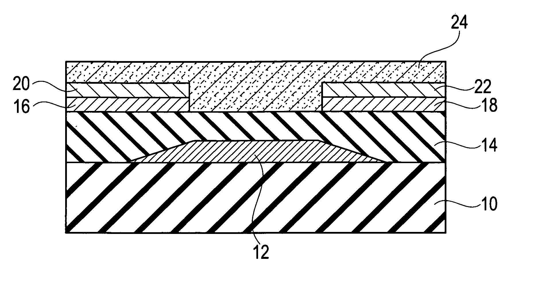
[0126]FIG. 5 shows a schematic cross-sectional configuration chart of an organic semiconductor device according to a first embodiment of the present invention. Moreover, FIG. 6 and FIG. 7 show an example of drain current ID-drain voltage VD characteristics and an example of drain current ID-gate voltage VG characteristics of the organic semiconductor device according to the first embodiment of the present invention, respectively.

[0127]As shown in FIG. 5, a structure of the organic semiconductor device according to the first embodiment of the present invention has an organic thin film transistor including: a substrate 10; a gate electrode 12 disposed on the substrate 10; a gate insulating film 15 disposed on the gate electrode 12; a gate insulating film 17 disposed on the gate insulating film 15; a source electrode (16, 20) and a drain electrode (18, 22) disposed on the gate insulating film 17 and composed of a layered structure of metal layers 16 and 18 and metal layers 20 and 22; a...

second embodiment

[0167]FIG. 8 shows a schematic cross-sectional configuration chart of an organic semiconductor device according to a second embodiment of the present invention. Moreover, FIG. 9 and FIG. 10 show an example of drain current ID-drain voltage VD characteristics and an example of drain current ID-gate voltage VG characteristics of the organic semiconductor device according to the second embodiment of the present invention, respectively.

[0168]As shown in FIG. 8, a structure of the organic semiconductor device according to the second embodiment of the present invention has an organic thin film transistor including: a substrate 10; a gate electrode 12 disposed on the substrate 10; a gate insulating film 15 disposed on the gate electrode 12; a gate insulating film 170 disposed on the gate insulating film 15; a source electrode (16, 20) and a drain electrode (18, 22) disposed on the gate insulating film 170 and composed of a layered structure of metal layers 16 and 18 and metal layers 20 and...

third embodiment

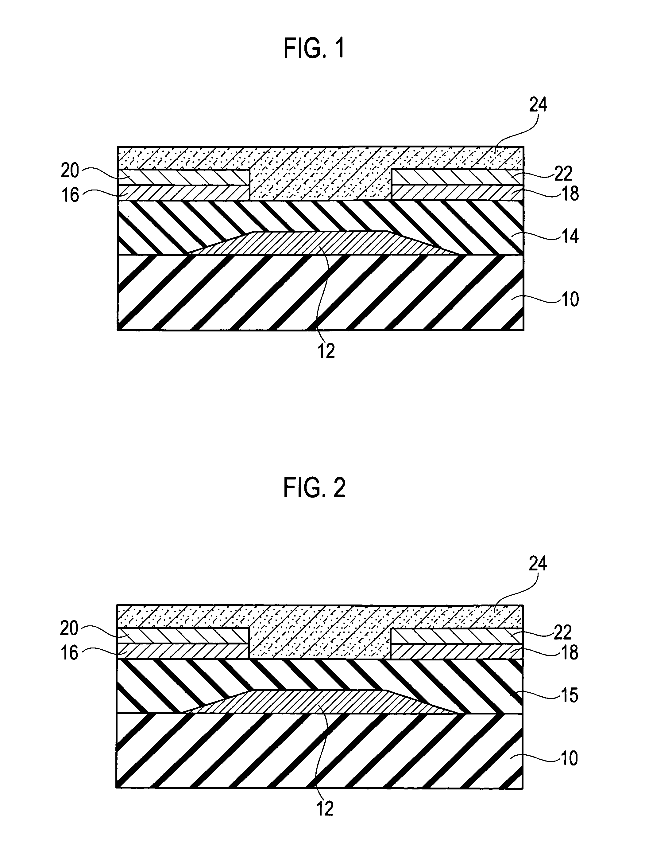
[0203]FIG. 15 shows a schematic cross-sectional configuration chart of an organic semiconductor device according to a third embodiment of the present invention.

[0204]As shown in FIG. 5, an organic semiconductor device according to the third embodiment of the present invention has an organic thin film transistor including: a substrate 10; a gate electrode 12 disposed on the substrate 10; a gate insulating film 13 disposed on the gate electrode 12; a gate insulating film 15 disposed on the gate insulating film 13; a gate insulating film 170 disposed on the gate insulating film 15; a source electrode (16, 20) and a drain electrode (18, 22) disposed on the gate insulating film 170 and composed of a layered structure of metal layers 16 and 18 and metal layers 20 and 22; and an organic semiconductor layer 24 disposed on the gate insulating film 170 and between the source electrode (16, 20) and the drain electrode (18, 22).

[0205]Moreover, the gate insulating film 15 may be composed of a ta...


PUM


Abstract

Provided is an organic semiconductor device, suitable for the integration, including an organic thin film transistor of low voltage drive and high driving current.
The organic semiconductor device including an organic thin film transistor comprising: a substrate (10); a gate electrode (12) disposed on the substrate (10); a first gate insulating film (15) disposed on the gate electrode (12); a second gate insulating film (17) disposed on the first gate insulating film (15); a source electrode (16, 20) and a drain electrode (18, 22) disposed on the second gate insulating film (17) and composed of a layered structure of a first metal layer (16, 18) and a second metal layer (20, 22); and an organic semiconductor layer (24) disposed on the gate insulating film (17) and between the source electrode (16, 20) and the drain electrode (18, 22). The first gate insulating film (15) is composed of an insulating film having a dielectric constant higher than that of the second gate insulating film (17), and the second gate insulating film (17) is composed of a silicon dioxide film thinner than the first gate insulating film (15), thereby providing a laminated type gate insulating film structure as a whole.

Description

TECHNICAL FIELD[0001]The present invention relates to an organic semiconductor device. In particular, the present invention relates to an organic semiconductor device which achieved improvement in transistor performance, by having a layered structure of a high dielectric constant insulating film and an ultra thin oxide film, or by using material with a larger work function for a source / drain electrode.BACKGROUND ART[0002]In a circuit element using an organic semiconductor, it is disclosed about a circuit element which keeps up characteristics of an organic semiconductor stabilizing for a long period of time, and is excellent in reliability with high endurance also for various stress, shocks, etc. from outside (for example, refer to Patent Literature 1). The circuit element according to Patent Literature 1 is characterized by a circuit element which forms a circuit unit including an organic semiconductor on a substrate, having a sealing canto surround the aforementioned circuit unit ...

Claims


Application Information

Patent Timeline
Patent Type & Authority Applications(United States)
IPC IPC(8): H01L51/10H01L51/30
CPCH01L51/0529H01L51/105H01L51/0545H10K10/474H10K10/84H10K10/466
Inventor OKU, YOSHIAKI
Owner ROHM CO LTD
Why Eureka
Try Eureka