
Sensitive field effect transistor apparatus

Active Publication Date: 2010-12-02
NOVASCOPE DIAGNOSTICS INC
View PDF2 Cites 1 Cited by
  • Summary
  • Abstract
  • Description
  • Claims
  • Application Information

AI Technical Summary

Benefits of technology

[0016]The Reference Field Effect Transistor of the invention comprises a semiconductor substrate of P-type silicon chip, wherein the P-well is formed in P-type silicon chip; the electrode formed by the source, drain, and P-type ion is formed in the P-well; the metal wire is connected to the surface of electrode; the silicon dioxide is formed on the surface of P-type silicon chip between the second electrode and metal wire; the single-layer silicon nitride is formed on the surface of P-well, it can reduce the sensitivity of hydrogen ion effectively, so that the surface will not be sensitive to hydrogen ion; the photo resistance layer is formed on the surface of silicon dioxide and the surface of metal wire to form the Reference Field Effect Transistor.
[0018]The invention integrates the Ion Sensitive Field Effect Transistor and Reference Field Effect Transistor in the same wafer. It is different from the prior art, which forms two independent elements. Thus the utilization is more convenient.
[0020]The invention can solve the problems of stability and service life of reference electrode encountered in the microminiaturization process. The differential amplifier can also be used to reduce the non-ideal effect of element.

Problems solved by technology

However, there still is a big problem to be solved in the manufacturing of micro Ion Sensitive Field Effect Transistor system.
This problem relates to the reference electrode.
However, the electrode stability and service life of these reference electrodes will be reduced due to the decrease of internal ion exchange solution under the microminiaturization process.
Thus, it is very difficult to microminiaturize the reference electrode.
It has seriously restrained the application and development of Ion Sensitive Field Effect Transistor on the biomedical field and human body inspection and diagnosis.
However, it is limited to the problem of membrane thickness.
When the membrane thickness is increased, the transconductance of element will be decayed, which will lead to the mismatch of system operation.
In addition, this kind of membrane has the stability and high sensitivity problems.3. Employ the polymer to form an ion-unblocking membrane.
Even so, the service life of this kind of membrane is still short.
However, there organic membrane and the semiconductor element still are the problems of complicated process and incompatible structure.

Method used


Image

  • Sensitive field effect transistor apparatus
  • Sensitive field effect transistor apparatus
  • Sensitive field effect transistor apparatus

Examples


Embodiment Construction

[0026]The invention selects the semiconductor process technology and uses the N-type or P-type semiconductor substrate, or the well to form the inorganic Ion Sensitive Field Effect Transistor / Reference Field Effect Transistor apparatus.

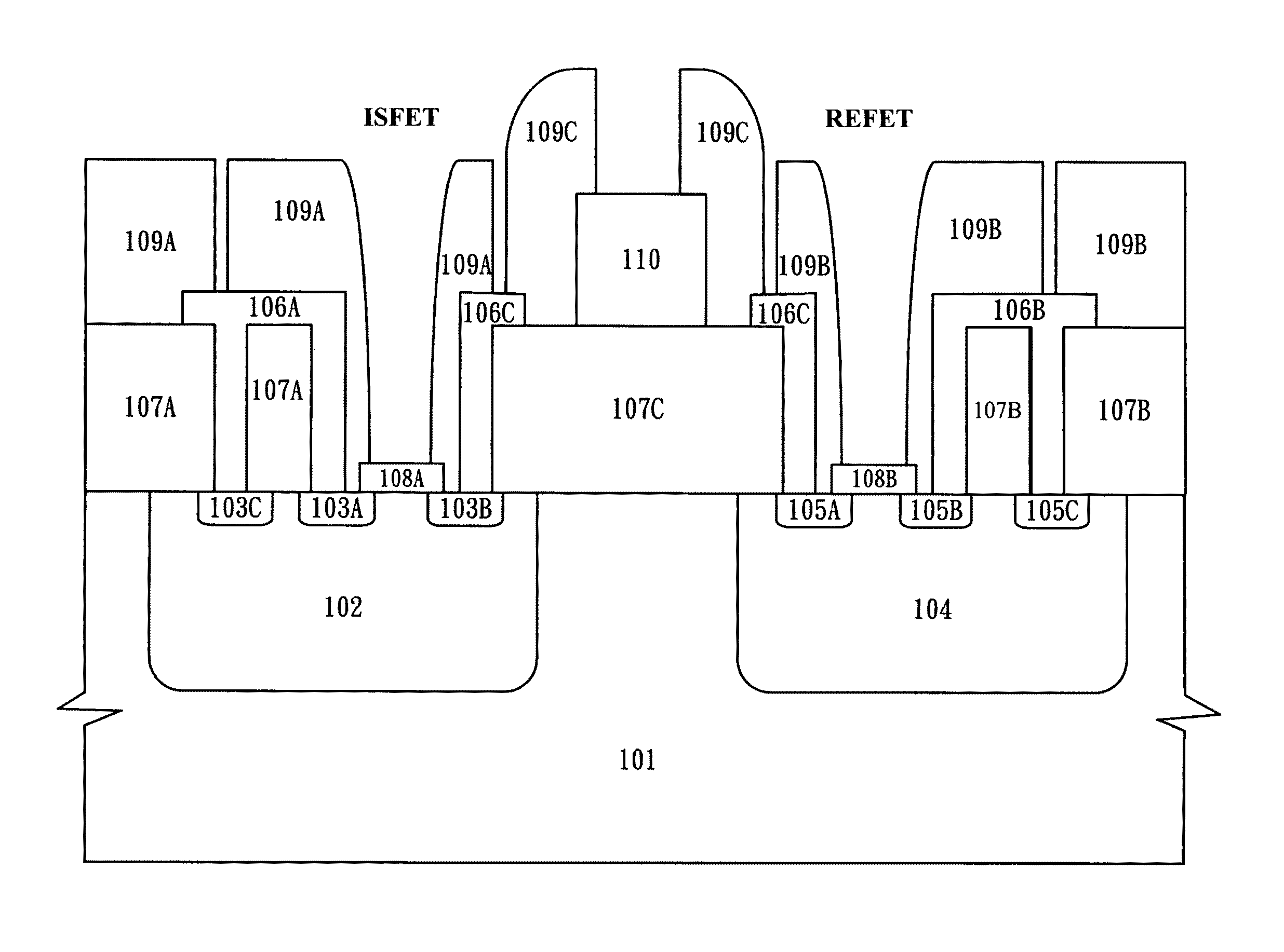
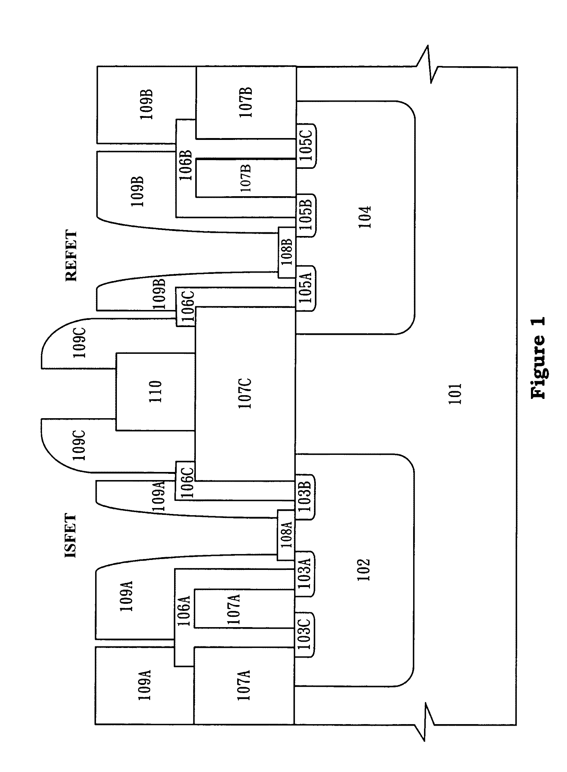
[0027]As shown in FIG. 1, a preferred embodiment of inorganic Ion Sensitive Field Effect Transistor / Reference Field Effect Transistor is illustrated, wherein the inorganic Ion Sensitive Field Effect Transistor (ISFET) is shown on the left hand side and the Reference Field Effect Transistor (REFET) is shown on the right hand side.

[0028]As shown in FIG. 1 again, the inorganic Ion Sensitive Field Effect Transistor on the left hand side comprises a semiconductor substrate of P-type silicon chip 101, the N-well 102 is formed in P-type silicon chip 101; the first electrode 103 formed in the N-well 102 is fabricated by the first source 103A, the first drain 103B, and N-type ion (N+) 103C. The first metal wire 106A is connected to the surface of the first ele...


PUM


Abstract

The invention discloses a sensitive field effect transistor apparatus, which uses the inorganic membrane to sense hydrogen ions. The invention adopts the membrane with high deformation stress. The sensitivity of sensitive membrane on hydrogen ion is adjusted through altering the membrane thickness and changing the substrate type and doped concentration. The differential amplifier is used to read signal to form the inorganic Ion Sensitive Field Effect Transistor / Reference Field Effect Transistor apparatus.

Description

BACKGROUND OF THE INVENTION[0001]1. Field of the Invention[0002]The invention relates to a Sensitive Field Effect Transistor apparatus, particularly to an Ion Sensitive Field Effect Transistor / Reference Field Effect Transistor / quasi Reference Electrode apparatus.[0003]2. Description of the Prior Art[0004]The initial concept of Ion Sensitive Field Effect Transistor (ISFET) was proposed by P. Bergveld in 1970 first. It has been improved and developed continuously. Since the development of Ion Sensitive Field Effect Transistor, the specific sensitive membrane material had been developed for many pH Ion Sensitive Field Effect Transistors (pH-ISFET). This material has high sensitivity and will not be interfered by non-ideal effect. In addition, due to the structure of Ion Sensitive Field Effect Transistor is similar to the structure of Metal-Oxide-Semiconductor Field Effect Transistor, the Complementary Metal Oxide Semiconductor (CMOS) process can be used to manufacture the Ion Sensitive...

Claims


Application Information

Patent Timeline
IPC IPC(8): H01L29/78
CPCG01N27/4148
Inventor LAI, CHAO-SUNGLUE, CHENG-ENYANG, CHIA-MINGWANG, SZU-CHIEH
Owner NOVASCOPE DIAGNOSTICS INC
Features
  • Generate Ideas
  • Intellectual Property
  • Life Sciences
  • Materials
  • Tech Scout
  • Unparalleled Data Quality
  • Higher Quality Content
  • 60% Fewer Hallucinations
Learn More