

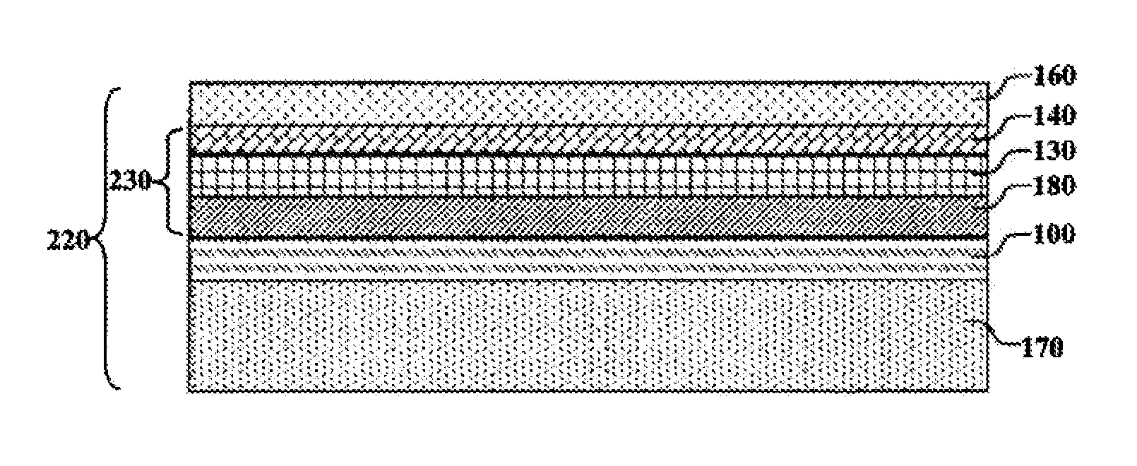
Inverted Bottom-Emitting OLED Device
a bottom-emitting, oled technology, applied in the direction of semiconductor devices, basic electric elements, electrical apparatus, etc., can solve the problems of low electron mobility in organic materials, high resistance of the medium, and the operation of the el device requires a high voltage (>100 volts) to achieve the effect of improving n-type semiconductor compatibility and reducing air sensitivity
- Summary
- Abstract
- Description
- Claims
- Application Information
AI Technical Summary
Benefits of technology
Problems solved by technology
Method used
Image

Examples
example 1
Comparative
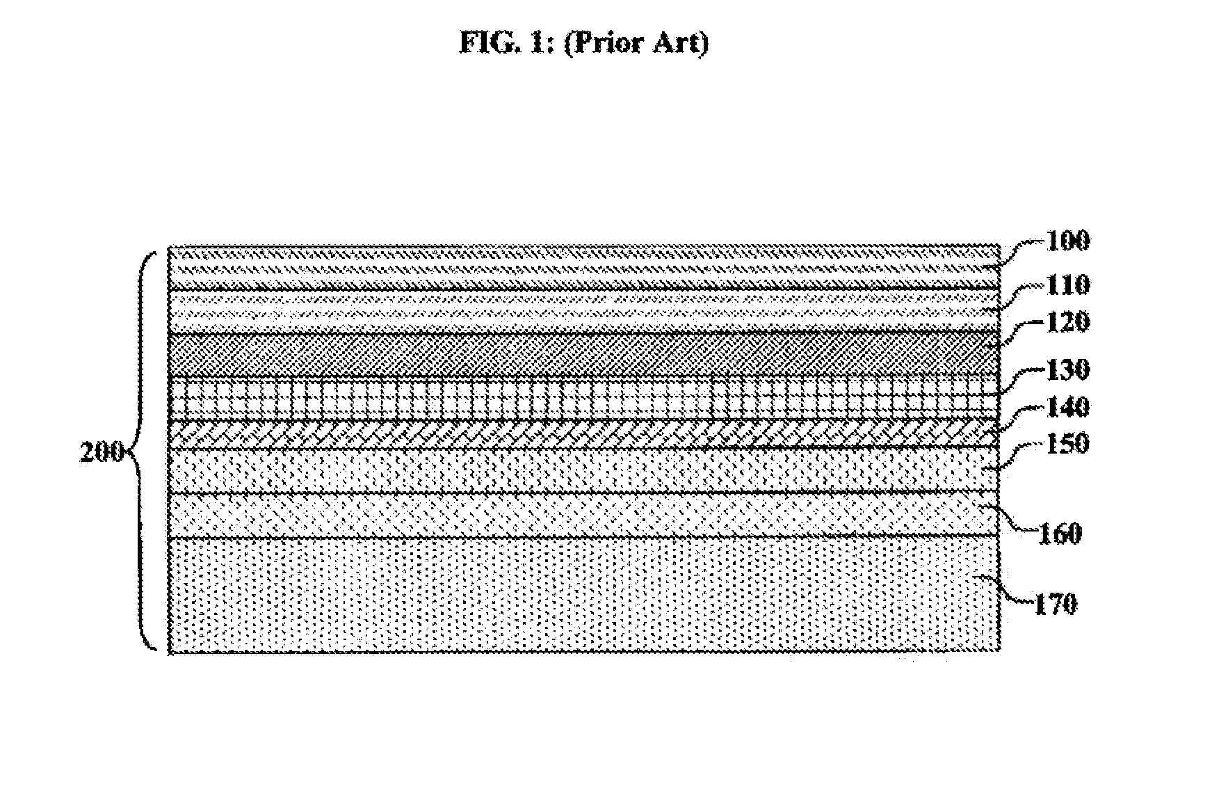
[0044]An OLED device was constructed in the following manner:[0045]1. A clean glass substrate with an ITO pattern was placed in a vacuum chamber and evacuated to 5×10⁻⁶ torr.[0046]2. The above-prepared substrate was treated by vacuum depositing a 60 nm including 94% 2-phenyl-9,10-bis(2-naphthyl)anthracene (PBNA) as host with 2% 4-(dicyanomethylene)-2-t-butyl-6-(1,1,7,7-tetramethyljulolidyl-9-enyl)-4H-pyran (DCJTB, a red dopant) as a light-emitting layer.[0047]3. The above-prepared substrate was further treated by vacuum-depositing a 120 nm layer of 4,4′-bis[N-(1-naphthyl)-N-phenylamino]biphenyl (NPB) as a hole-transporting layer.[0048]4. The above-prepared substrate was further treated by vacuum-depositing a 10 nm layer of hexacyanohexaazatriphenylene (CHATP) as a hole-injecting layer (HIL).
[0049]5. A 60 nm silver anode layer was deposited onto the sample by vacuum evaporation.
example 2
Inventive
[0050]An OLED device was constructed as described in Example 1, except that the following step was added between Steps 1 and 2:[0051]1a. A 40 nm layer of unpatterned ZnO was deposited uniformly on the substrate.
[0052]After deposition, a positive voltage was applied to the top (anode) electrode and a negative voltage to the bottom (cathode) electrode at a constant current of 20 ma / cm2. Any spectral output was measured. Example 1, the comparative example did not emit. Inventive Example 2 emitted orange light with a spectral maximum at 593 nm wavelength and a luminance of 61 candela / m2. This shows that the zinc oxide layer, which is an electron-transporting layer, enables this device to function.
example 3
Comparative
[0053]An OLED device was constructed in the following manner:[0054]1. A clean glass substrate with an ITO pattern was placed in a vacuum chamber and evacuated to 5×10⁻⁶ torr.[0055]2. The above-prepared substrate was treated by vacuum depositing a 40 nm PBNA layer with 0.75% green-emitting dopant GED-1 as a light-emitting layer.
[0056]3. The above-prepared substrate was further treated by vacuum-depositing a 75 nm layer of NPB as a hole-transporting layer.[0057]4. A 10 nm hole-injecting layer of CHATP was vacuum-deposited onto the substrate at a coating station.[0058]5. A 40 nm silver anode layer was deposited onto the sample by vacuum evaporation.[0059]6. A 30 nm aluminum conductive protective layer was deposited onto the sample by vacuum evaporation.
PUM
 Abstract
Description
Claims
Application Information