Another complex example is the production of
multiple layer printed circuit boards allowing much more complex circuits than were ever possible with single or
dual layer materials.
The first methodology allows materials and devices of
high complexity to be manufactured, but at high cost.
Further deficiencies and impediments in these methods create production compromises which further hinder attainment of the goal of low cost
mass production of complex layered devices.
Attempts have been made to combine these processes to achieve these aims but with varying and limited success.
Most of these approaches to materials or device fabrication are limited to creating 2-dimensional or 2%-dimensional structures.
The most common of these approaches use one or more of Computer
Numerical Control (CNC) micromilling, injection-molding or
hot embossing, which can generate only very limited feature complexity.
However, these are serial fabrication processes that have alignment challenges when assembling micro-parts which lead to further labor-intensive processes with relatively low
throughput and high associated production costs.
However, this is a more difficult proposition for reel-to-reel systems where the
production line is a continuous process.
Although U.S. Pat. No. 4,805,111 describes a modularized
web system that can allow reconfiguration of the line, the flexibility of the
system and the complexity of the produced devices are limited due to the continuous nature of the supply feed of the source materials when the
system is in use.
These
batch manufacturing technologies, however, are rather expensive, especially when involving micro-features.
The main industrial applications of devices made according to such methods are in high-
throughput-oriented products in large industrial, scientific and governmental laboratories where the component can be reused, therefore the cost is amortized over the device's operational lifespan.
For many potential applications of miniaturized layered bio-analytical devices, especially in disposable parts for point-of-care / point-of-use devices, such high production costs cannot be justified.
However due to the technical challenge of
miniaturization and the need for such devices to reliably interface to real world samples and instruments, layered polymeric devices made this way are typically larger than their
silicon or glass counterparts and provide unique packaging challenges.
Furthermore, these batch-based processes can be difficult to automate, making the storing, handling, aligning and assembling of the produced micro-parts a commercial and technical challenge in itself.
Consequently the number of devices that can be economically fabricated in parallel from a
polymer batch-based process is restricted, making this method suitable for only
low volume production.
Whereas each of these processes, widely used in industry, are optimized for high
throughput, and several
automation strategies to link serial processes are well in place for conventional products, the cycle times, the complexity and the cost of the necessarily highly automated process sequences all increase significantly for micro-structured devices.
Storing, handling, assembling and aligning micro-parts in a competitive industrial environment remain the technical and economical challenges.
Such web-based production lines tend to be highly automated and therefore very labor-efficient.
Although initial investment costs for a web-based
production line are higher than for serial production, manufacturing costs per product can be very low for a suitable large-scale
production line.
The main
disadvantage of such reel-to-reel production lines is that they are typically very sensitive to process variations.
If a single
processing component on the line goes out of tolerance or fails, then, due to the continuous nature of the production line, all parts passing that point are affected and production is effectively curtailed.
Stopping the line to fix the problematic part causes the entire production run to come to a halt.
The lines are typically dedicated to one specific product, and require large investments in setup time and optimization of parameters, particularly when dealing with the tight tolerance requirements for devices with micro-features.
Due to this setup time, the lengths of the web systems and the total effect of misalignment due to
wear and tear or component failure, there is typically a lot of material waste.
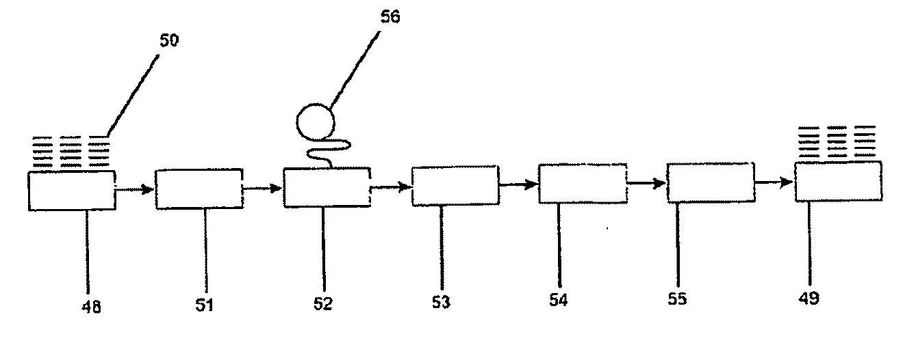
Another
disadvantage of a reel-to-reel
system is that the slowest process in the system limits the speed of the whole production system.
This limits the thickness of the
layers used and the number of
layers that can be combined and still be handled in such a production line.
This presents problems for many layered material applications that require larger interfaces to the environment, larger fluid capacities, large handling structures, or a higher degree of component strength, or large numbers of bonded layers all of which characteristics tend to make the
resultant device very rigid and therefore severely
restrict the suitability of a reel-to-reel production method.
Another
disadvantage of reel-to-reel handling systems is that the substrates need to remain in a mostly planar form with external surfaces having little or no protuberances.
As the substrate thickness is also limited by this method, this imposes further design constraints on the product, which often require larger 3-dimensionally shaped objects to provide functionality, such as
interfacing to an external device or the provision of internal
liquid storage compartments.

