

FIB Process for Selective and Clean Etching of Copper
a selective and clean etching technology, applied in vacuum evaporation coatings, sputtering coatings, coatings, etc., can solve the problems of difficult to achieve clean uniform fib etching of copper for ce, non-uniform and uneven fib etching of copper, and rough surface of etched copper, etc., to prevent electrical short circuit, low volatility, and high stickiness
- Summary
- Abstract
- Description
- Claims
- Application Information
AI Technical Summary
Benefits of technology
Problems solved by technology
Method used
Image

Examples
Embodiment Construction
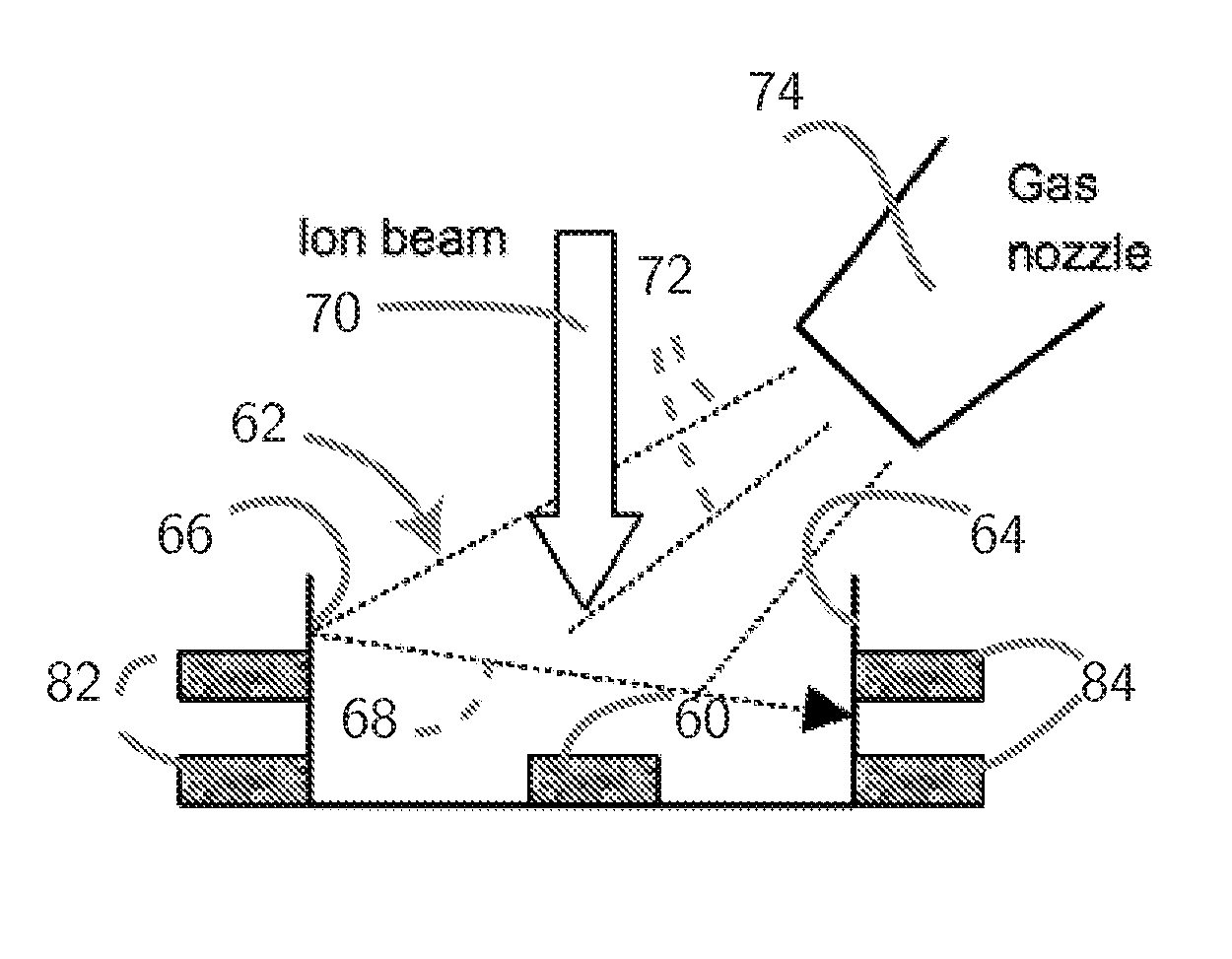
[0026]The invention is particularly well adapted to the focused ion beam (FIB) etching of copper interconnects, power and ground planes and the like in ICs for circuit editing (CE), and will be described in that context. However it will be appreciated that this is illustrative of only one utility of the invention, and that the invention has greater applicability.
[0027]Conventional FIB apparatus and operations are well known and will not be described in detail herein. U.S. Pat. No. 7,060,196, which is hereby incorporated by reference herein, discloses FIB apparatus that uses Gallium (Ga+) ions for milling copper over organic dielectrics in a context and environment similar to that of the present invention, and such FIB apparatus may be used to practice the invention.
[0028]Although conventional FIB apparatus and processes have typically employed Gallium (Ga+) ions, different metal ions, non-metal ions, noble gas ions and molecular ions may also be used advantageously in FIB processes....
PUM
| Property | Measurement | Unit |
|---|---|---|
| Temperature | aaaaa | aaaaa |
| Temperature | aaaaa | aaaaa |
| Temperature | aaaaa | aaaaa |
Abstract
Description
Claims
Application Information