Semiconductor device and method of manufacturing the same

a technology of semiconductor and spherical fin, which is applied in the direction of semiconductor devices, transistors, electrical devices, etc., can solve the problems of difficult to meet, difficult to perform a uniform and high concentration implantation of impurities into the side surface of the fin, and the sidewall becomes a hindrance factor, etc., to achieve the effect of improving the parasitic resistan

Active Publication Date: 2011-03-03
RENESAS ELECTRONICS CORP
View PDF7 Cites 64 Cited by
  • Summary
  • Abstract
  • Description
  • Claims
  • Application Information

AI Technical Summary

Benefits of technology

[0014]The following explains briefly the effect acquired by the typical invention among the inventions disclosed in the present application.
[0015]In FINFETs, it is possible to achieve the improvement of the parasitic resistance.

Problems solved by technology

The miniaturization of the MISFET has been advanced in a style conforming to the scaling law, but, with respective progresses of the device generation, various problems have appeared, and it becomes difficult to satisfy both the suppression of the short channel effect and the securement of a high-current driving capability of the MISFET.
On this occasion, since the sidewall is formed on the side wall of the fin, it becomes difficult to perform a uniform and high concentration implantation of impurities into the side surface of the fin.
Furthermore, the sidewall becomes a hindrance factor when siliciding the surface of the fin.
This makes it difficult to achieve the improvement of parasitic resistance at the side surface of the fin.

Method used


Image

  • Semiconductor device and method of manufacturing the same
  • Semiconductor device and method of manufacturing the same
  • Semiconductor device and method of manufacturing the same

Examples


example 1

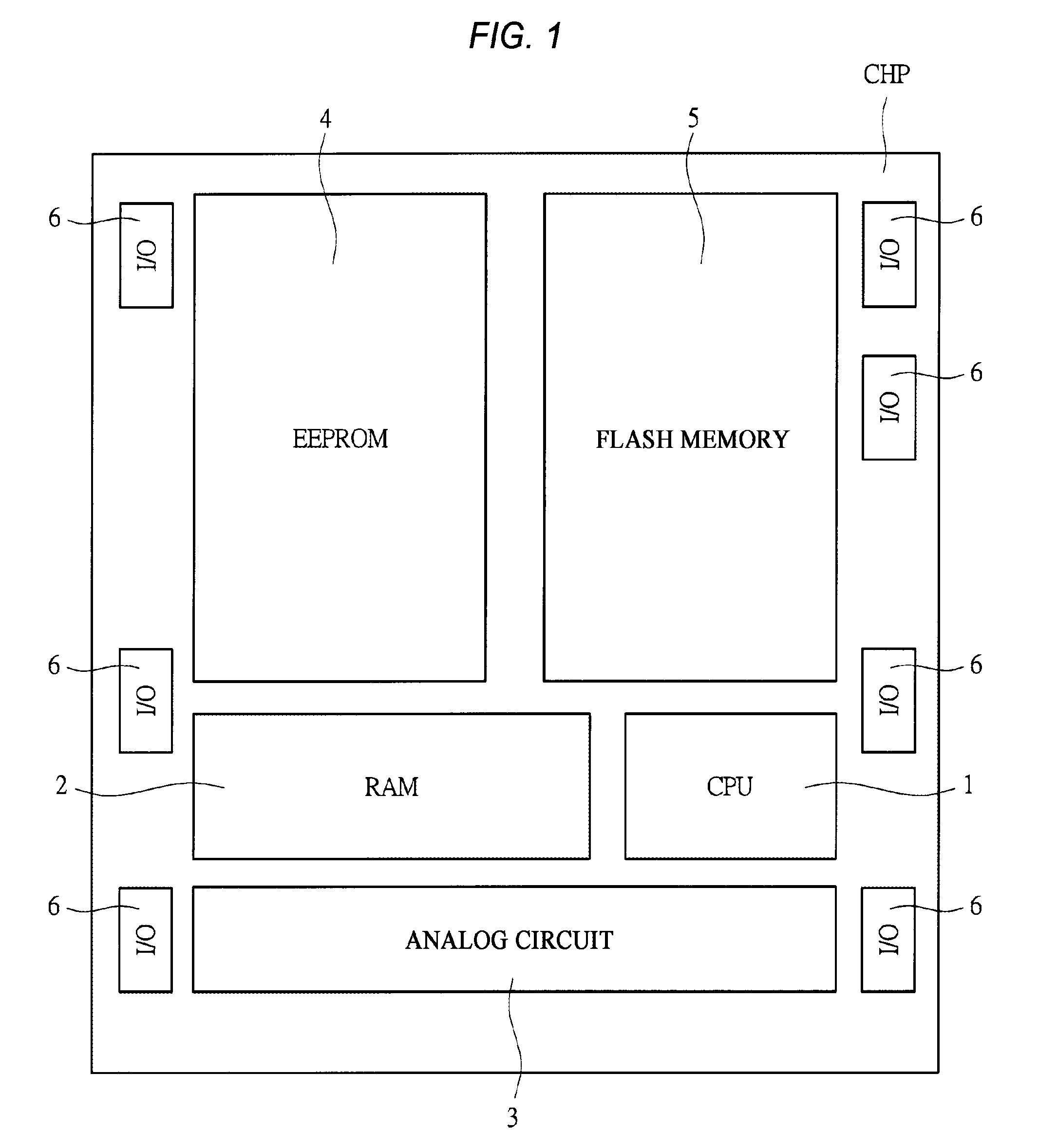
[0059]A semiconductor device in the present Example 1 will be described with reference to the drawing. Firstly, the layout configuration of a semiconductor chip, in which a system including a microcomputer is formed, is described. FIG. 1 is a drawing showing the layout configuration of a semiconductor chip CHP in Example 1. In FIG. 1, the semiconductor chip CHP has a CPU (Central Processing Unit) 1, a RAM (Random Access Memory) 2, an analog circuit 3, an EEPROM (Electrically Erasable Programmable Read Only Memory) 4, a flash memory 5 and an I / O (Input / Output) circuit 6.

[0060]The CPU (the circuit) 1 is also referred to as a central processing unit, which corresponds to the heart portion of computers and the like. The CPU 1 reads out an instruction from a memory device and decodes it, and, on the basis of it, performs various calculation or control.

[0061]The RAM (the circuit) 2 is a memory capable of randomly reading out memory information, that is, reading out stored memory informati...

example 2

[0166]In the Example 1, the example, in which the sidewall SW is formed from the laminated film including the silicon oxide film OX1, the silicon nitride film SN1 and the silicon oxide film OX2, is explained, but, in Example 2, an example, in which the sidewall SW is formed from the silicon nitride film, silicon oxide film and silicon nitride film, is explained.

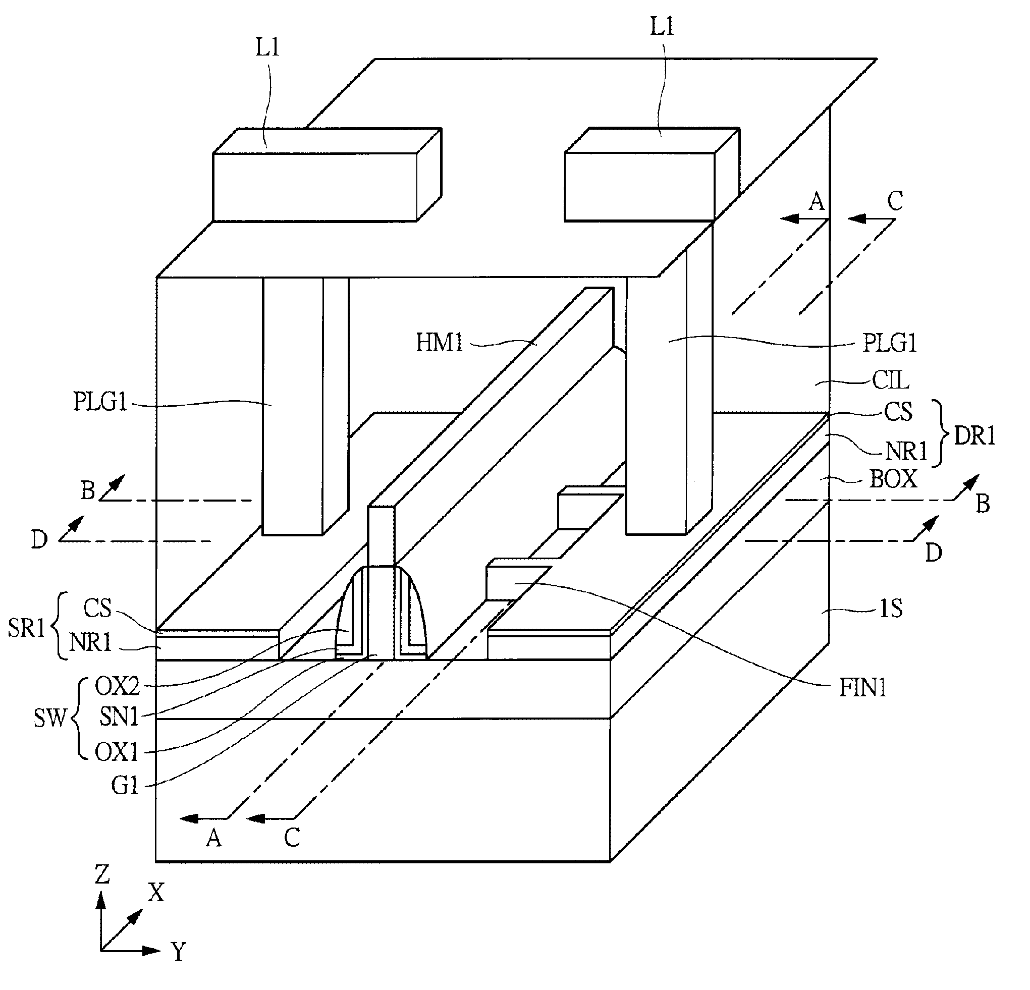
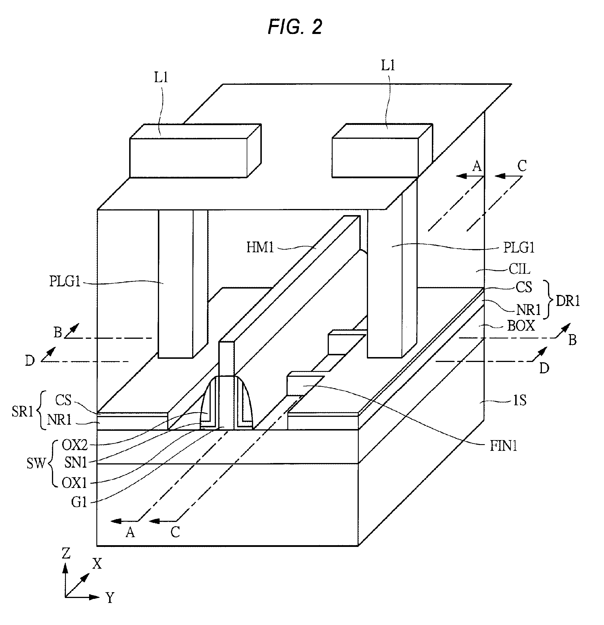
[0167]FIG. 32 is a drawing showing the positional relation between the fin FIN1 and the gate electrode G1 constituting the FINFET. As shown in FIG. 32, the fin FIN1 extends in the X direction, but, on the other hand, the gate electrode G1 extends in the Y direction. In addition, the gate electrode G1 is disposed in a region intersecting the fin FIN1 so as to cross over the fin FIN1. On side walls on both sides of the gate electrode G1 extending in the Y direction, the sidewall SW is formed. In Example 2, the sidewall SW is constituted by the silicon nitride film SN1 formed over the side wall of the gate electrode G1, the sili...

example 3

[0173]In the above Example 1, as shown in FIGS. 27 to 29, after removing the silicon oxide film OX1 formed in the lowermost layer and forming the sidewall SW, the high concentration n-type impurity diffusion regions NR1 and NR2, and the deep n-type impurity diffusion region NR3 are formed. That is, after removing the silicon oxide film OX1, the ion implantation method is practiced to form the high concentration n-type impurity diffusion regions NR1 and NR2, and the deep n-type impurity diffusion region NR3.

[0174]In contrast, in Example 3, an example, in which the silicon oxide film OX1 formed in the lowermost layer is left and the ion implantation method is practiced to form the high concentration n-type impurity diffusion regions NR1 and NR2, and the deep n-type impurity diffusion region NR3, is explained.

[0175]As shown in FIG. 27, the silicon oxide film OX1 in the lowermost layer constituting the sidewall SW is not removed but left. After that, via the left silicon oxide film OX1,...


PUM

PropertyMeasurementUnit
thicknessaaaaaaaaaa
thicknessaaaaaaaaaa
thicknessaaaaaaaaaa

Abstract

To provide a technique capable of achieving improvement of the parasitic resistance in FINFETs. In the FINFET in the present invention, a sidewall is formed of a laminated film. Specifically, the sidewall is composed of a first silicon oxide film, a silicon nitride film formed over the first silicon oxide film, and a second silicon oxide film formed over the silicon nitride film. The sidewall is not formed on the side wall of a fin. Thus, in the present invention, the sidewall is formed on the side wall of a gate electrode and the sidewall is not formed on the side wall of the fin.

Description

CROSS-REFERENCE TO RELATED APPLICATION[0001]The disclosure of Japanese Patent Application No. 2009-201594 filed on Sep. 1, 2009 including the specification, drawings and abstract is incorporated herein by reference in its entirety.BACKGROUND OF THE INVENTION[0002]The present invention relates to a semiconductor device and a technique of manufacturing the same, particularly to a technique that is effective when applied to a semiconductor device including a FINFET (FIN Field Effect Transistor) and a technique of manufacturing the same.[0003]Japanese Patent Laid-Open No. 2008-10790 (Patent Document 1) describes a technique that relates to FINFETs. In particular, a sidewall is formed on the side wall of a gate electrode constituting the FINFET, and the sidewall is also formed on the side wall of the fin. The document explains that the sidewall is formed of a laminated film of silicon oxide film / silicon nitride film / silicon oxide film.[0004]Japanese Patent Laid-Open No. 1988-182866 (Pate...

Claims


Application Information

Patent Timeline
Patent Type & Authority Applications(United States)
IPC IPC(8): H01L27/088H01L21/762
CPCH01L21/76243H01L27/1211H01L21/845H01L21/76256H01L27/1207
Inventor ISHIKAWA, KOZOSHINOHARA, MASAAKIIWAMATSU, TOSHIAKI
Owner RENESAS ELECTRONICS CORP
Why Eureka
Try Eureka