

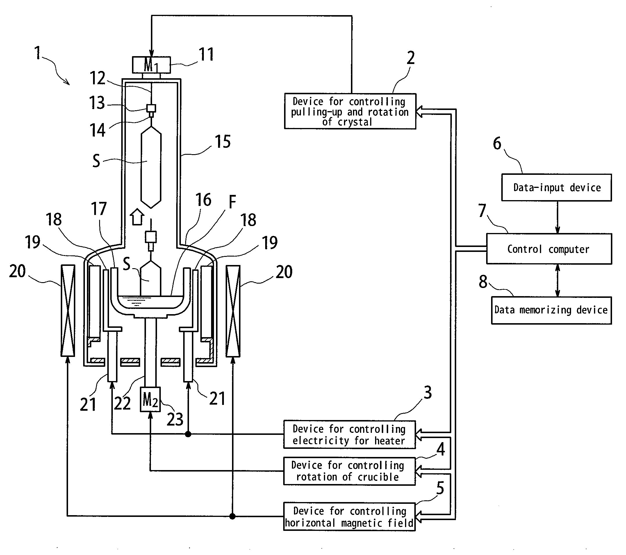
Method of producing single crystal silicon
a single crystal silicon and production method technology, applied in the direction of polycrystalline material growth, crystal growth process, polycrystalline material growth, etc., can solve the problems of disturbing single crystallization, achieve low resistivity, avoid cell growth, and produce reliably
- Summary
- Abstract
- Description
- Claims
- Application Information
AI Technical Summary
Benefits of technology
Problems solved by technology
Method used
Image

Examples
Embodiment Construction
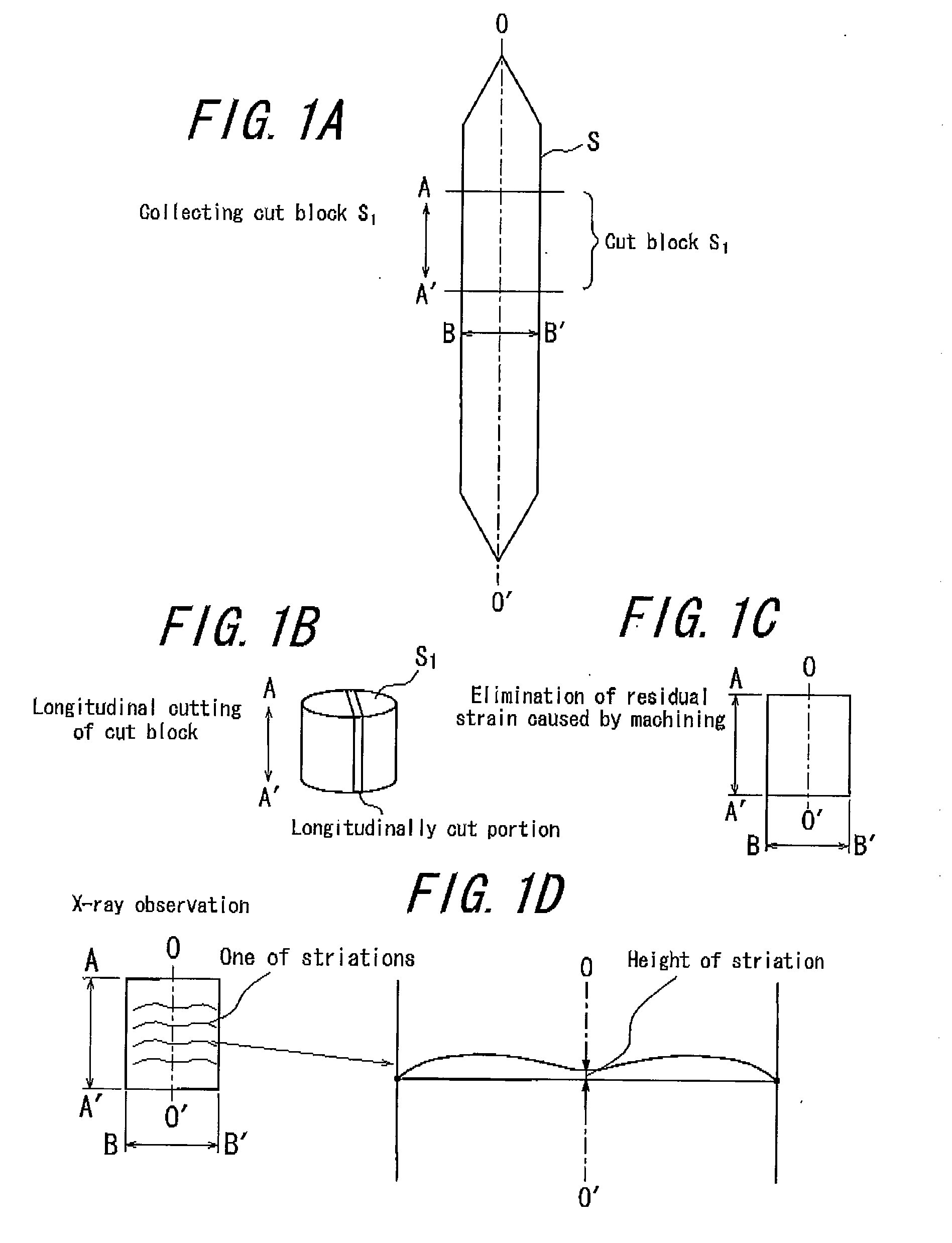
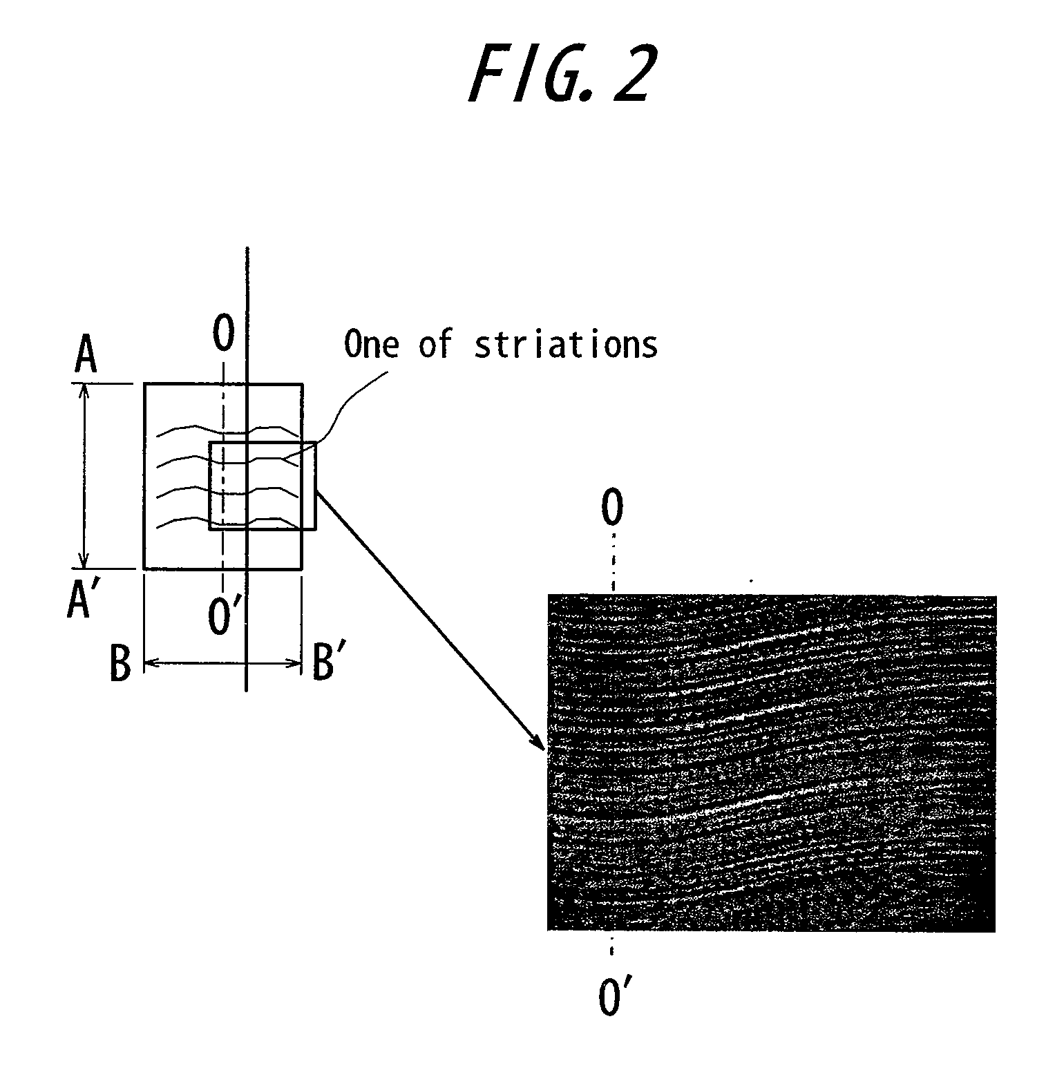
[0025]As described above, the inventors of the present invention paid particular attention to striations distinctively appearing in an impurity-doped crystal and contrived the present invention on the basis of the results of a keen study regarding correlation between these striations and presence / absence of cell growth. The results of experiments which led to the present invention will be described in detail hereinafter. First, striations in each of ingots obtained under various production conditions are examined. Specifically, as shown in FIG. 1A, a single crystal silicon ingot is cut at predetermined sites, for example, A-A′ and B-B′ shown in the drawing, whereby a cut block S1 is obtained.
Next, as shown in FIG. 1B, the cut block S1 is further cut along the longitudinal axis O-O′ of the original ingot, whereby a longitudinally cut portion is collected.
[0026]Next, as shown in FIG. 1C, the longitudinally cut portion thus collected is subjected to an etching process such that residua...
PUM
| Property | Measurement | Unit |
|---|---|---|
| resistivity | aaaaa | aaaaa |
| diameter | aaaaa | aaaaa |
| diameter | aaaaa | aaaaa |
Abstract
Description
Claims
Application Information