
Resin composition for optical semiconductor device, optical-semiconductor-device lead frame obtained using the same, and optical semiconductor device

a semiconductor device and semiconductor technology, applied in the direction of thermoelectric devices, optical elements, instruments, etc., can solve the problems of reducing the efficiency of light reflection, and achieve excellent heat resistance of soldering, excellent properties, and high thermal discoloration resistance

Inactive Publication Date: 2011-03-10
NITTO DENKO CORP
View PDF7 Cites 14 Cited by
  • Summary
  • Abstract
  • Description
  • Claims
  • Application Information

AI Technical Summary

Benefits of technology

[0023]The present inventors diligently made investigations in order to obtain a resin composition for optical semiconductor packages which is inhibited from suffering thermal deformation or discoloration and is excellent in soldering heat resistance, long-term high-temperature heat resistance, and light degradation resistance. As a result, they have found that use of a thermosetting resin composition including an epoxy resin in combination with a polyorganosiloxane makes it possible to attain a combination of the excellent properties possessed by the epoxy resin and the high thermal discoloration resistance and light degradation resistance which are characteristics of the polyorganosiloxane and renders fabrication with a mold by, for example, transfer molding possible. This is advantageous also from the standpoint of suitability for mass production. The desired objects are thus accomplished, and the invention has been achieved.
[0024]As shown above, the invention provides a resin wall for an optical semiconductor package which includes a metallic lead frame or substrate and an optical semiconductor element mounted thereon, in which the resin wall is formed around the circumference of the optical semiconductor element, the resin wall being formed from a material for resin wall formation which includes the resin composition including an epoxy resin [ingredient (A)], a curing agent [ingredient (B)], a polyorganosiloxane [ingredient (C)], and a white pigment [ingredient (D)]. Because of this, the resin wall is excellent in soldering heat resistance and long-term high-temperature heat resistance, exhibits excellent performance also with respect to light degradation resistance, and renders excellent light-reflecting properties possible. Consequently, in an optical semiconductor device obtained using the resin composition for forming the resin wall, an excellent light reflectivity attributable to the resin wall is maintained over a long period of time, and hence, the resin wall can sufficiently perform the function thereof.
[0025]When the cured material obtained from the resin composition has a light reflectivity of 80% or higher at a wavelength of 450 nm to 800 nm, it is possible to lower the power of the light-emitting element while maintaining the same brightness with respect to light of each color, owing to the high reflectivity. As a result, the effect of retaining heat resistance regarding high-temperature discoloration, etc. can be prolonged. In addition, thermal decreases in adhesion to encapsulating resins and thermal deformation of encapsulating resins can be prevented.
[0026]When the content of the polyorganosiloxane [ingredient (C)] is in the range of 5 to 60% by weight based on all organic components including the ingredients (A) to (C), not only even better heat resistance and light degradation resistance are obtained but also a excellent cured resin composition is obtained.
[0027]When titanium oxide is used as the white pigment [ingredient (D)], excellent whiteness and light-reflecting properties are obtained because titanium oxide has excellent dispersibility, chemical stability, etc.
[0028]Furthermore, when an inorganic filler is used together with those ingredients, a reduction in the liner expansion coefficient and a further improvement in flowability are realized.

Problems solved by technology

Consequently, although there are desires for thermal deformation resistance at soldering temperatures, for thermal discoloration resistance, and for heat resistance for longer period of time required due to increases in the power of optical semiconductor elements 2, use of the thermoplastic resins results in discoloration, etc. at high temperatures and this poses problems such as a decrease in the efficiency of light reflection.

Method used


Image

  • Resin composition for optical semiconductor device, optical-semiconductor-device lead frame obtained using the same, and optical semiconductor device
  • Resin composition for optical semiconductor device, optical-semiconductor-device lead frame obtained using the same, and optical semiconductor device
  • Resin composition for optical semiconductor device, optical-semiconductor-device lead frame obtained using the same, and optical semiconductor device

Examples


examples

[0083]Examples are given below together with Comparative Examples. However, the invention should not be construed as being limited to the following Examples.

[0084]First, prior to the production of resin compositions, the ingredients shown below were prepared.

[0085]Epoxy Resin a1: Triglycidyl isocyanurate (epoxy equivalent: 100)

[0086]Epoxy Resin a2: Bisphenol A diglycidyl ether (epoxy equivalent: 450)

[0087]Acid Anhydride Methylhexahydrophthalic anhydride (acid equivalent: 168)

[0088]Polyorganosiloxane c1

[0089]Into a flask were introduced 206 g (50 mol %) of phenyltrimethoxysilane and 126 g (50 mol %) of dimethyldimethoxysilane. A mixture of 1.2 g of 20% aqueous HCl solution and 40 g of water was added dropwise thereto. After completion of the dropwise addition, refluxing was continued for 1 hour. Subsequently, the resultant solution was cooled to room temperature (25° C.) and then neutralized with sodium hydrogen carbonate. The organosiloxane solution obtained was filtered to remove i...


PUM

PropertyMeasurementUnit
light reflectivityaaaaaaaaaa
reflectivityaaaaaaaaaa
softening pointaaaaaaaaaa

Abstract

The present invention relates to a resin composition for optical semiconductor devices, the resin composition including the following ingredients (A) to (D): (A) an epoxy resin; (B) a curing agent; (C) a polyorganosiloxane; and (D) a white pigment.

Description

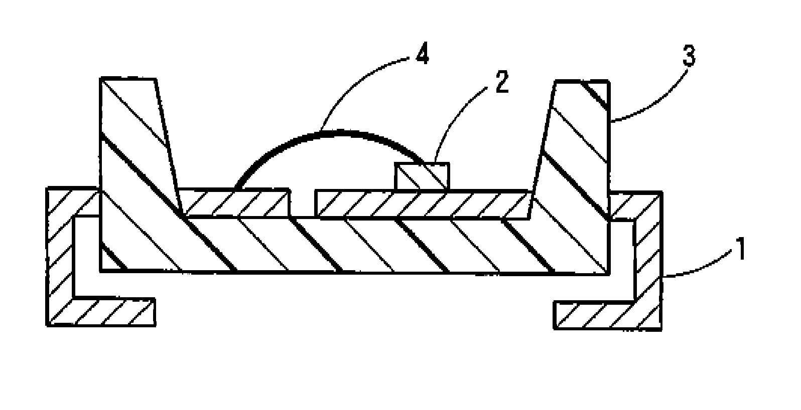
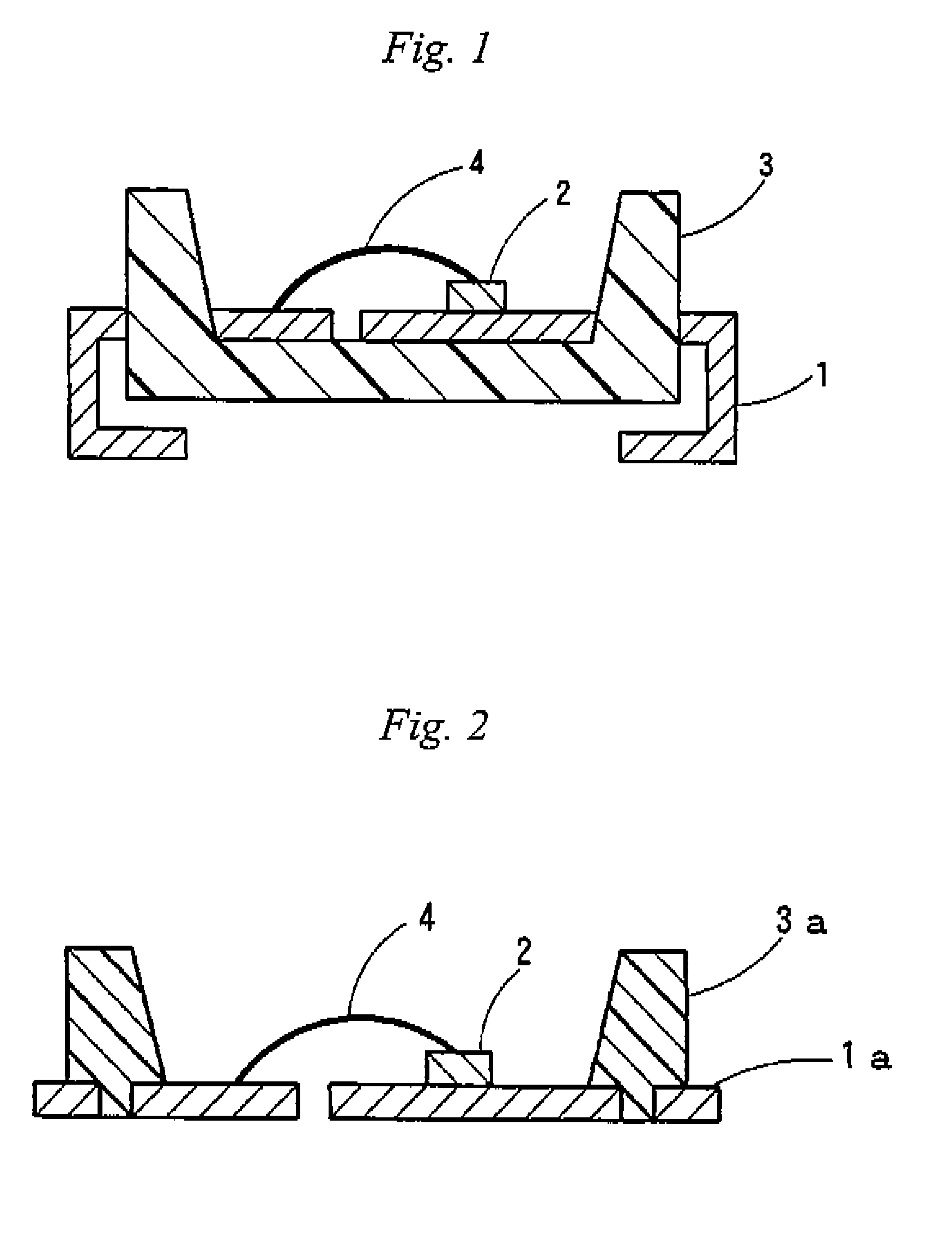
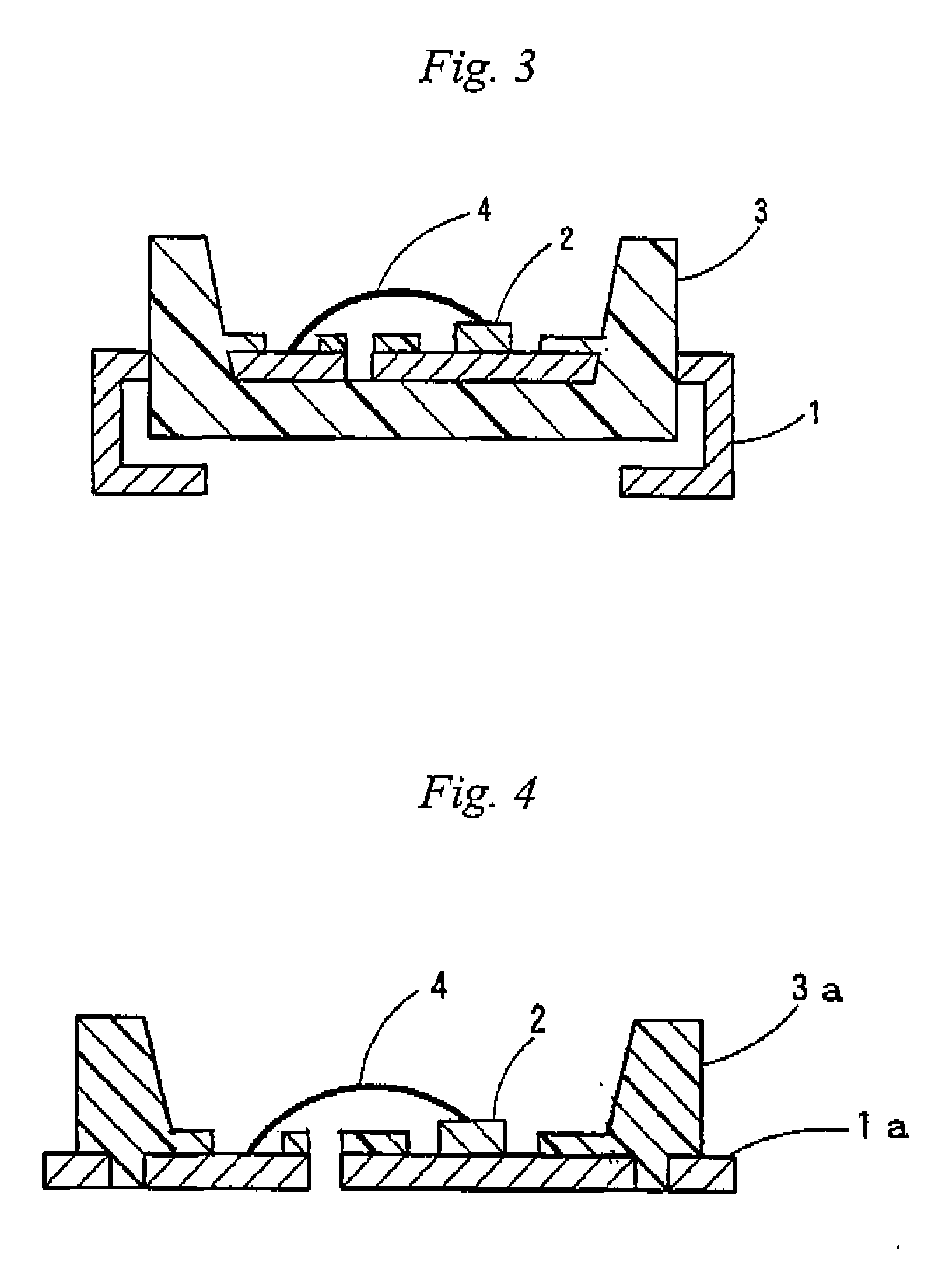
FIELD OF THE INVENTION[0001]The present invention relates to a resin composition for optical semiconductor devices which serves as a material for forming a resin layer around an optical semiconductor element, and relates to an optical-semiconductor-device lead flame obtained using the resin composition and an optical semiconductor device.BACKGROUND OF THE INVENTION[0002]Conventional optical semiconductor devices including an optical semiconductor element mounted therein, for example, have a configuration including a metallic lead frame 1, an optical semiconductor element 2 mounted thereon, and a resin wall formed from a resin layer 3 so as to surround the circumference of the optical semiconductor element 2, as shown in FIG. 1. In FIG. 1, numeral 4 denotes a bonding wire which electrically connects an electrode circuit (not shown) formed on the metallic lead frame 1 to the optical semiconductor element 2, the bonding wire being disposed according to need.[0003]When such an optical s...

Claims


Application Information

Patent Timeline
Patent Type & Authority Applications(United States)
IPC IPC(8): G02B6/36C08L63/00C08K3/22
CPCC08G59/3245C08G59/4215C08L63/00H01L2224/48247H01L2224/48091C08L83/04H01L2924/00014C08K3/22C09C1/62H01L33/62
Inventor TANIGUCHI, TAKASHIFUKE, KAZUHIRONORO, HIROSHIITO, HISATAKA
Owner NITTO DENKO CORP
Learn More