
Large capacity solid-state storage devices and methods therefor

a solid-state storage, large-capacity technology, applied in the direction of memory adressing/allocation/relocation, generating/distributing signals, instruments, etc., can solve the problems of limiting the overall capacity of the device to a much smaller size, prohibitive cost of nand flash memory, and limited capacity of current solid-state drives (ssds)

Inactive Publication Date: 2011-03-10
OCZ STORAGE SOLUTIONS
View PDF7 Cites 34 Cited by
  • Summary
  • Abstract
  • Description
  • Claims
  • Application Information

AI Technical Summary

Benefits of technology

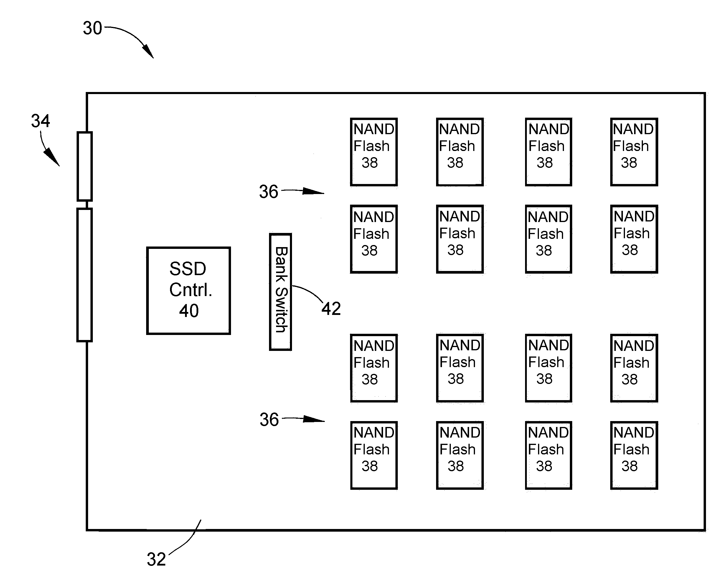
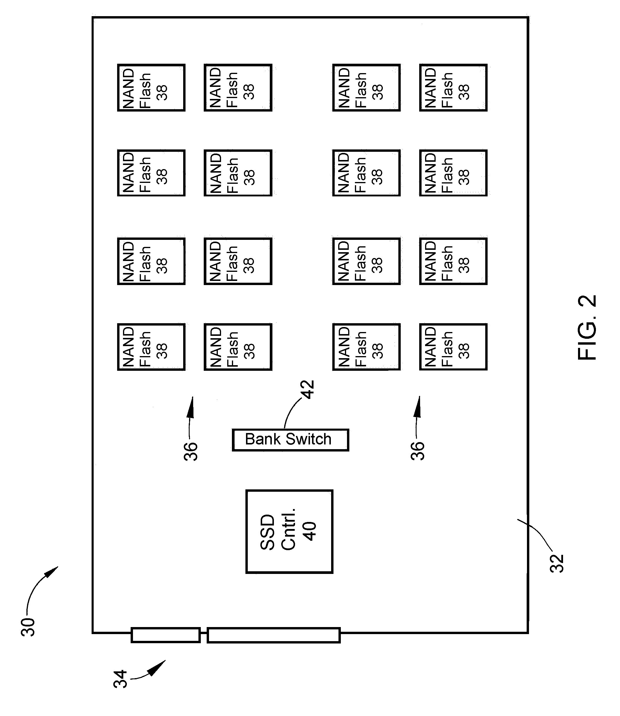
[0013]From the above it can be appreciated that, according to certain aspects of the invention, a large capacity SSD can be provided that is capable of using a single conventional SSD controller. In combination with the bank switching circuitry, the controller can be operated to translate a small address space into several physical address spaces, each using its own bank of memory devices. As a result, a significant advantage made possible with this invention is that the desired capacity of an SSD can exceed the addressing space of its memory controller.

Problems solved by technology

Current solid state drives (SSDs) are limited in their capacity by the density of the NAND chips in conjunction with the limitations of the control logic, that is, the memory controller.
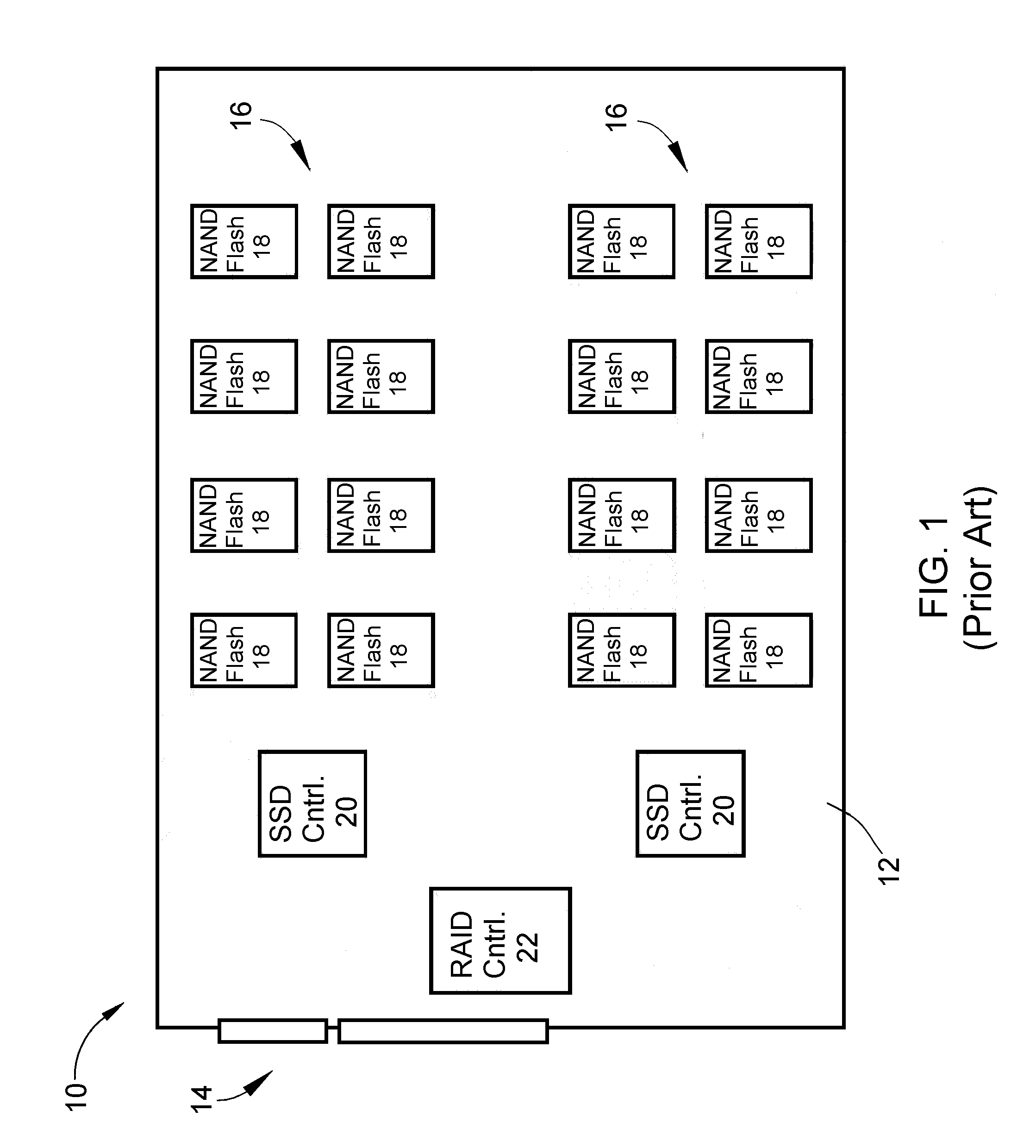
Even if the memory management unit is aware of a large memory space through, for example, a 48-bit large block addressing scheme, the actual controller will typically have limitations in the number of address lines or chip-selects, which then limits the overall capacity of the device to a much smaller size.
In the past, the cost of NAND flash memory was prohibitive for even considering ultra-high capacity solid state drives, but with production ramping up and NAND cost decreasing on average by 50% per year, SSDs have not only gained acceptance in the market but are also constantly increasing in capacity.
Functionally, the RAID 0, as the most commonly used, will not be able to play out the combined transfer rates of two drives because the system interface (connector 14) is usually a single SATA link, which limits the host transfer rate and can cause some problems if the combined internal media transfer rate at the back-end of the SSD 10 is greater than the host transfer rate.

Method used


Image

  • Large capacity solid-state storage devices and methods therefor
  • Large capacity solid-state storage devices and methods therefor
  • Large capacity solid-state storage devices and methods therefor

Examples


Embodiment Construction

[0020]The present invention is generally applicable to computers and other processing apparatuses, and particularly to personal computers, workstations and other apparatuses that utilize nonvolatile (permanent) memory-based mass storage devices, a notable example of which are solid-state drives (SSDs) that make use of NAND flash memory devices. FIGS. 2 and 3 schematically represent SSDs configured as internal mass storage devices for a computer or other host system (not shown) equipped with a data and control bus for interfacing with the SSDs. The bus may operate with any suitable protocol in the art, a preferred example being the serial advanced technology attachment (SATA) bus, though other protocols are also possible.

[0021]FIG. 2 shows an SSD 30 as comprising a printed circuit board 32 equipped with a power and data connector 34 and separate banks 36 of memory devices 38 according to one embodiment of the invention. The memory devices 38 are non-volatile memory devices, preferabl...


PUM


Abstract

Non-volatile storage devices and methods capable of achieving large capacity SSDs containing multiple banks of memory devices. The storage devices include a printed circuit board, at least two banks of non-volatile solid-state memory devices, bank switching circuitry, a connector, and optionally a memory controller. The bank switching circuitry is functionally interposed between the banks of memory devices and either the connector or the memory controller. The bank switching circuitry operates to switch accesses by a system logic or the memory controller among the at least two banks.

Description

CROSS REFERENCE TO RELATED APPLICATIONS[0001]This application claims the benefit of U.S. Provisional Application No. 61 / 240,338, filed Sep. 8, 2009, the contents of which are incorporated herein by reference.BACKGROUND OF THE INVENTION[0002]The present invention generally relates to memory devices for use with computers and other processing apparatuses. More particularly, this invention relates to high capacity non-volatile or permanent memory-based mass storage devices of the type known as solid state drives (SSD).[0003]Mass storage devices such as advanced technology (ATA) or small computer system interface (SCSI) drives are rapidly adopting non-volatile memory technology such as flash memory or other emerging solid state memory technology, including phase change memory (PCM), resistive random access memory (RRAM), magnetoresistive random access memory (MRAM), ferromagnetic random access memory (FRAM), organic memories, or nanotechnology-based storage media such as carbon nanofibe...

Claims


Application Information

Patent Timeline
IPC IPC(8): G06F12/02G06F12/00G06F1/12
CPCG06F3/0626G06F3/0658G06F2212/7208G06F12/0246G06F3/0679
Inventor SCHUETTE, FRANZ MICHAEL
Owner OCZ STORAGE SOLUTIONS
Learn More