Organic Electroluminescence Device

an electroluminescence device and organic technology, applied in the direction of solid-state devices, discharge tubes/lamp details, natural mineral layered products, etc., can solve the problem that the aromatic amine derivatives disclosed in u.s. patent no. 6,815,090 do not have sufficient lighting efficiency, and achieve low luminance efficiency and better luminance efficiency

Active Publication Date: 2011-03-31
RITDISPLAY
View PDF1 Cites 21 Cited by
  • Summary
  • Abstract
  • Description
  • Claims
  • Application Information

AI Technical Summary

Benefits of technology

[0012]In comparison with low luminance efficiency of the devices of prior arts, the present invention can provide an organic electroluminescence device with similar colors and better luminance efficiency.

Problems solved by technology

However, because electroluminescence devices do not have backlight units, they must include a self-contained light source.
The aromatic amine derivatives disclosed in U.S. Pat. No. 6,815,090 do not have sufficient lighting efficiency.

Method used


Image

  • Organic Electroluminescence Device
  • Organic Electroluminescence Device
  • Organic Electroluminescence Device

Examples


first embodiment

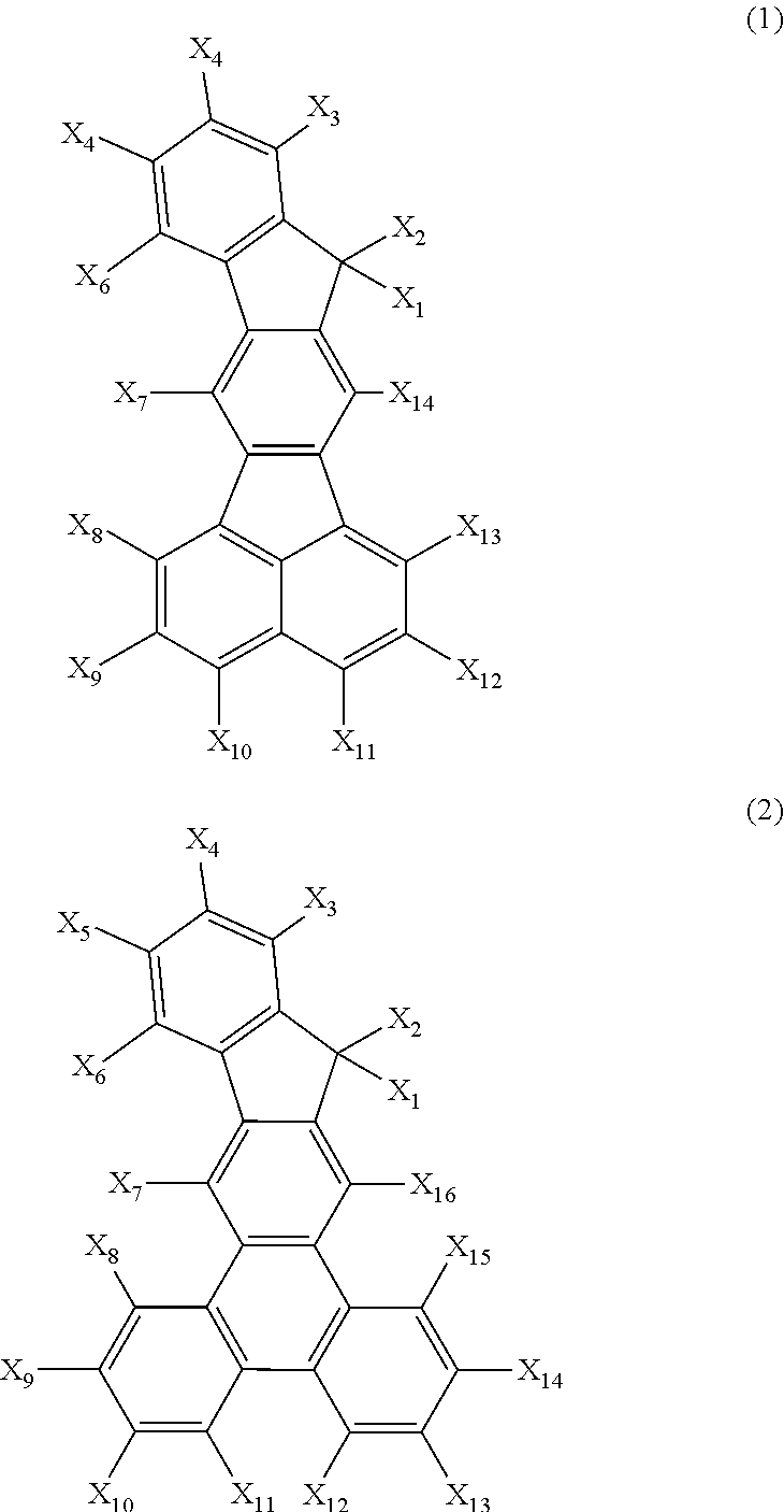
[0025]Y1 shows a fluorescent compound in accordance with a first embodiment of the present invention.

[0026]The organic electroluminescence device may be manufactured as follows:

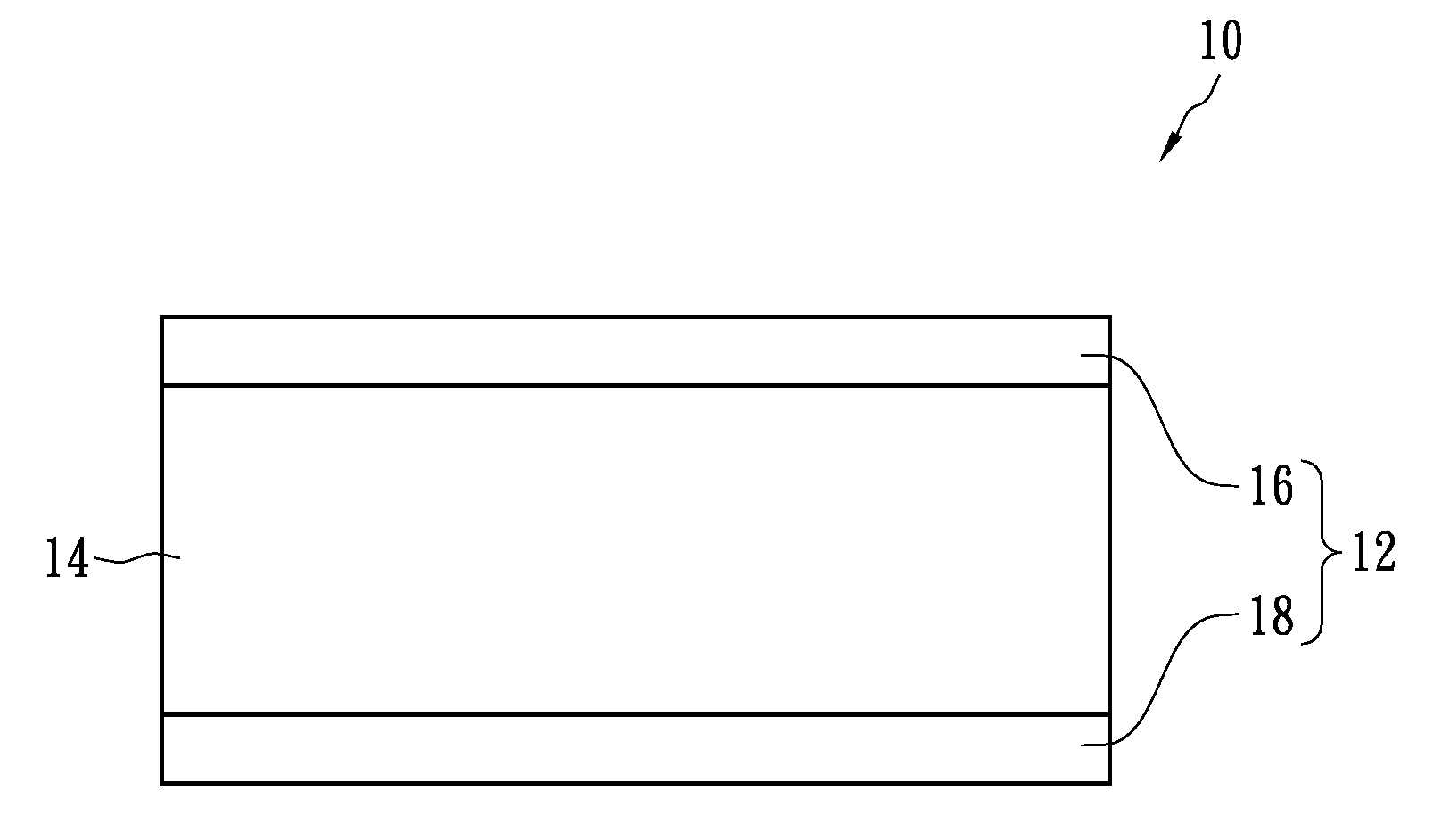
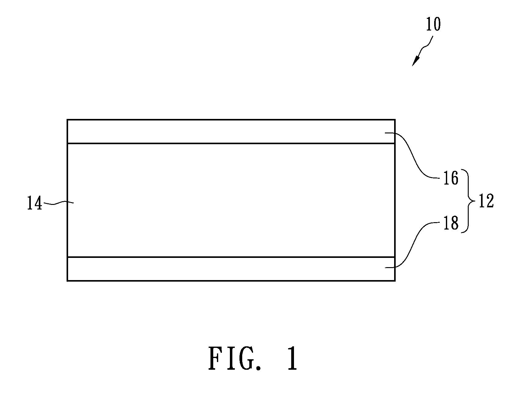
[0027]First, a glass substrate is provided, and an indium tin oxide (ITO) layer of 150 nm is disposed on the glass substrate with an area of 100 mm×100 mm. After forming a pattern on the 10 mm×10 mm lighting area by lithography, the device is subjected to vacuum evaporation deposition at 10−5 Pa, so as to form a hole transporting layer NPB (N,N′-bis-(1-naphthyl)-N,N′-diphenyl-(1,1′-biphenyl)-4,4′-diamine) of 65 nm with a deposition rate of 0.2 nm / sec. Next, ADN((9,10-Di(naphth-2-yl)anthracene) and Y1 are deposited to form an light-emitting layer of 40 nm, in which compound Y1 is 4% of ADN, and the vapor deposition rate is 0.2 nm / sec. Next, AlQ3 (tris(8-quinolino)aluminum) is deposited as an electron transporting layer of 15 nm with a vapor deposition rate of 0.2 nm / sec. Lastly, lithium fluoride with a thickne...

embodiment 2

[0028]Y2 shows a fluorescent compound in accordance with a second embodiment of the present invention.

[0029]The organic electroluminescence device is manufactured according to the method of that shown in Embodiment 1, but with Y1 replaced by Y2.

embodiment 3

[0030]Y3 shows a fluorescent compound in accordance with a third embodiment of the present invention:

[0031]The organic electroluminescence device is manufactured according to the method for that shown in Embodiment 1, but with Y1 replaced by Y3.


PUM

PropertyMeasurementUnit
thicknessaaaaaaaaaa
thicknessaaaaaaaaaa
fluorescentaaaaaaaaaa

Abstract

An organic electroluminescence device includes an organic layer disposed between at least one pair of electrodes, wherein the organic layer includes at least one fluorescent compound selected from compounds represented by the following general formulae (1) and (2):
    • wherein X1 to X16 each independently represents a hydrogen atom, a linear, branched or cyclic alkyl group having 1 to 20 carbon atoms, a linear, branched or cyclic alkoxy group having 1 to 20 carbon atoms, a substituted or unsubstituted aryl group having 6 to 30 carbon atoms, a substituted or unsubstituted aryloxy group having 6 to 30 carbon groups, a substituted or unsubstituted arylamino group having 6 to 30 carbon atoms, a substituted or unsubstituted alkylamino group having 1 to 30 carbon atoms, a substituted or unsubstituted arylalkylamino group having 7 to 30 carbon atoms or a substituted or unsubstituted alkenyl group having 8 to 30 carbon atoms; a pair of adjacent groups represented by X1 to X2 and a pair of adjacent substituents to groups represented by X1 to X2 may form a cyclic structure in combination; a pair of adjacent groups represented by X3 to X16 and a pair of adjacent substituents to groups represented by X3 to X16 may form a cyclic structure in combination; when the pair of adjacent substituents are aryl groups, the pair of substituents may be a single group; and in the formulae at least one of the substituents of X3 to X14 or X16 includes amino group.

Description

BACKGROUND OF THE INVENTION[0001](A) Field of the Invention[0002]The present invention relates to an organic electroluminescence (EL) device, and particularly to an organic electroluminescence device of aromatic amine derivative.[0003](B) Description of the Related Art[0004]Electroluminescence is a lighting phenomenon in which currents flow through a material or a material is disposed in high-voltage electrical fields. Electroluminescence is also known in industry as “cold light.” Electroluminescence devices may be zinc sulfide and blue diamond doped with copper or silver. Current development efforts in the electroluminescence field are focused on the application of organic materials.[0005]Organic light-emitting diodes (OLED) with electroluminescence features use display technologies in which light is generated by current-driven organic semiconductor materials and lighting materials, so as to display images. In comparison with liquid crystal displays (LCD), the organic light-emittin...

Claims


Application Information

Patent Timeline
Patent Type & Authority Applications(United States)
IPC IPC(8): H01L51/54
CPCC09K11/06H05B33/14C09K2211/1011
Inventor TSENG, SHIH PINCHEN, MING LEISU, CHENG FENG
Owner RITDISPLAY
Why Eureka
Try Eureka