
Layered product having porous layer and functional layered product made with the same

a technology of functional layered products and porous layers, which is applied in the direction of dielectric characteristics, conductive pattern formation, instruments, etc., can solve the problems of reducing the shielding effect, requiring an expensive production apparatus, and affecting the operation of the operator of the instrument, etc., and achieves excellent flexibility of the porous layer, excellent folding endurance and handling ability, and sufficient strength

Inactive Publication Date: 2011-04-07
DAICEL CHEM IND LTD
View PDF7 Cites 27 Cited by
  • Summary
  • Abstract
  • Description
  • Claims
  • Application Information

AI Technical Summary

Benefits of technology

[0064]In the layered product having the porous layer of the present invention, the average pore diameter of the micropores in the porous layer and the porosity of the layer are each set in the specified range, so that the flexibility of the porous layer is excellent. Additionally, the porous layer is sufficient in strength and excellent in folding endurance and handleability since the porous layer is backed with the base.
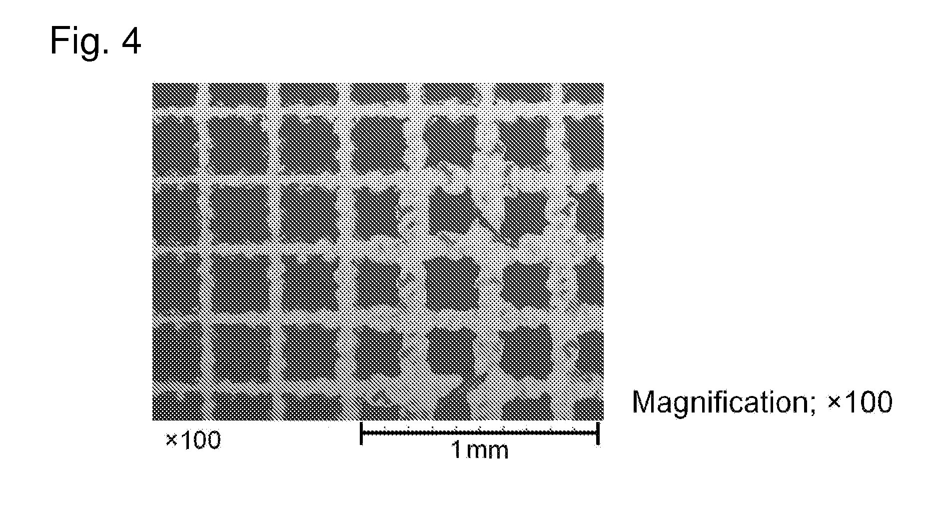
[0065]Since the layered product having the porous layer of the present invention has the above-mentioned characteristics, the layered product is excellent in printability onto porous layer surface thereof so that a fine functional pattern made of a conductor material or the like can be printed thereon. Further, the composition constituting the porous layer has a glass transition temperature of 20° C. or higher; therefore, when the composition is subjected to a heat treatment, the porous layer softens so that the micropores disappear. Thus, the porous layer can be converted to a transparent layer the film thickness of which is decreased. In word words, when a fine functional pattern is printed on the porous layer surface and subsequently the pattern-printed layered product is subjected to a heat treatment, a fine functional pattern can be obtained on the resultant transparent resin layer. It is generally difficult to print a fine pattern made of a conductor material or the like directly onto a transparent resin layer because the resin layer has denseness (the resin layer has a nature of being poor in cushioning performance, and being smooth). Against this point, therefore, the present invention has a great advantage.
[0066]As described above, the layered product having the porous layer of the present invention is used to make it possible to yield a functional layered product wherein a fine functional pattern made of a conductor material or the like is formed on a base by interposition of a transparent resin layer originating from the porous layer. When a light-transmitting base is used as the base, a functional layered product that is transparent as a whole can be obtained. The resultant functional layered product can be broadly used as a substrate material including an electromagnetic wave controlling material such as an electromagnetic wave shield or an electromagnetic wave absorbent, a circuit substrate, an antenna, and a heat sink plate.
[0067]According to the present invention, through simple steps of printing a fine functional pattern onto the surface of the porous layer, and subjecting, after the printing, the resultant layered product to a heat treatment, it is possible to yield, at low production costs, a functional layered product wherein a functional pattern is formed on the base by interposition of a transparent resin layer originating from the porous layer.

Problems solved by technology

It is pointed out that EMI causes malfunctions or troubles of the surrounding electronic or electric instruments, and further gives health problems to operators of these instruments.
However, when the electro-conductive layer is made as thin as the layer can attain transparency, the surface resistance of the electro-conductive layer becomes too large so as to cause a problem that the shielding effect is declined.
Moreover, the use of the vapor deposition technique requires an expensive production apparatus, and generally gives poor productivity.
Thus, a problem that costs for the production increase is caused.
However, the fiber diameter of the electro-conductive fiber, which is 35 μm (in paragraph of JP 5-327274A) or 76 μm (in paragraph of JP 5-269912 A), is too large; therefore, the fiber is unfavorably seen.
Thus, the EMI shielding material is unsuitable for being used as a display.
Thus, an expensive production apparatus is necessary, and the production efficiency is poor because of a long and complicated production step.
Therefore, a problem that production costs increase remains.

Method used


Image

  • Layered product having porous layer and functional layered product made with the same
  • Layered product having porous layer and functional layered product made with the same
  • Layered product having porous layer and functional layered product made with the same

Examples


example 1

Porous Layer-Layered Product

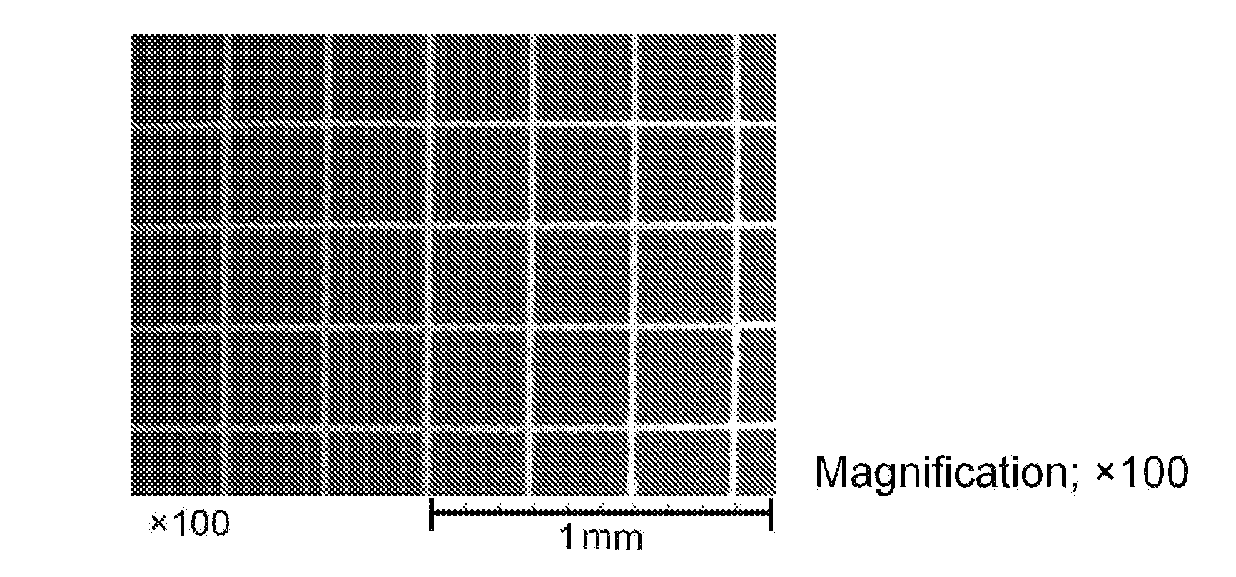
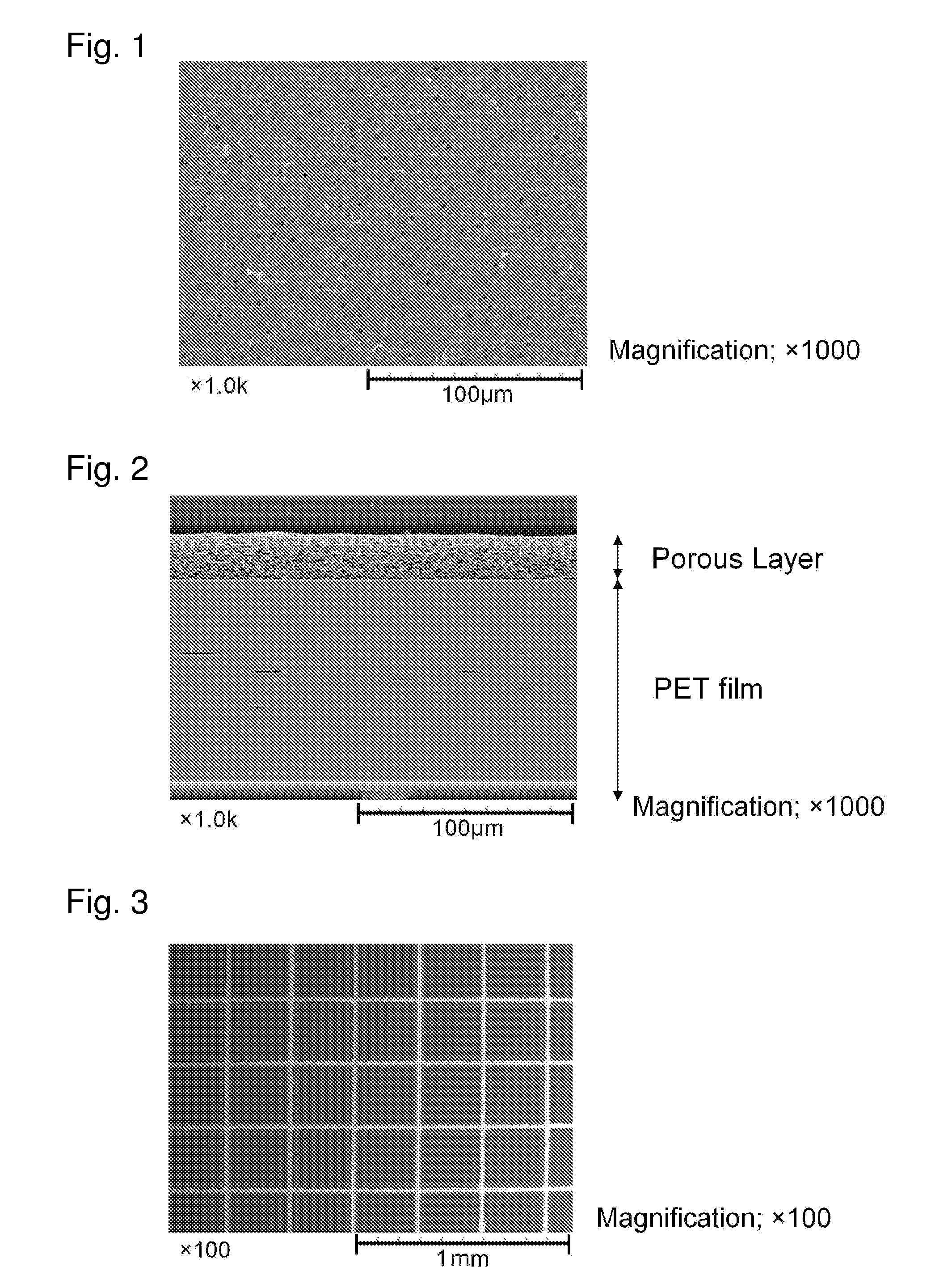
[0246]A polyvinyl butyral resin solution (“POLYVINYL BUTYRAL 2400” manufactured by Wako Pure Chemical Industries, Ltd. (average polymerization degree: about 2,300 to 2,500); solid content concentration: 15% by weight; solvent: NMP) was prepared, and this was used as a material solution for film-formation. A PET film (S type; thickness: 100 μm) manufactured by Teijin DuPont Films Japan Limited as a base was fixed onto a glass plate with a tape. This material solution, the temperature of which was set to 25° C., was cast onto the base using a film applicator under a condition that the gap between the film applicator and the base was 76 μm. Immediately after the casting, the resultant article was kept in a vessel having a humidity of about 100% and a temperature of 50° C. for 4 minutes. Thereafter, the article was immersed in water to be coagulated. Next, the article was naturally dried at a room temperature without peeling the cast material from the base, t...

example 2

Porous Layer-Layered Product

[0248]To 100 parts by weight of a polyvinyl butyral resin solution (“POLYVINYL BUTYRAL 2400” manufactured by Wako Pure Chemical Industries, Ltd. (average polymerization degree: about 2,300 to 2,500); solid content concentration: 15% by weight; solvent: NMP) was added 10 parts by weight of polyethylene glycol 400 (average molecular weight: 360 to 440) manufactured by Wako Pure Chemical Industries, Ltd. as a water-soluble polymer, so as to prepare a material solution for film-formation. A PET film (S type; thickness: 100 μm) manufactured by Teijin DuPont Films Japan Limited as a base was fixed onto a glass plate with a tape. This material solution, the temperature of which was set to 25° C., was cast onto the base using a film applicator under a condition that the gap between the film applicator and the base was 102 μm. Immediately after the casting, the resultant article was kept in a vessel having a humidity of about 100% and a temperature of 50° C. for 4...

example 3

Porous Layer-Layered Product

[0250]The same operations as in Example 2 were made except that a PET film (trade name: “LUMIRROR T60” manufactured by Toray Industries, Inc.; thickness: 100 μm) was used instead of the PET film (S type; thickness: 100 μm) manufactured by Teijin DuPont Films Japan Limited as a base in Example 2, so as to yield a layered product C wherein a white porous layer was layered on the base. The thickness of the resultant porous layer was about 15 μm, and the total thickness of the layered product was about 115 μm.

[0251]About the obtained layered product C, the tape peeling test was made. As a result, no interfacial peeling was caused between the base and the porous layer. This layered product C was observed with an electron microscope. As a result, the porous layer adhered closely to the PET film, and was substantially homogenous inside thereof, and had micropores having an average pore diameter of about 2 μm over the whole thereof. The porosity inside the porous...


PUM

PropertyMeasurementUnit
porosityaaaaaaaaaa
pore diameteraaaaaaaaaa
glass transition temperatureaaaaaaaaaa

Abstract

The present invention provides a layered product having a porous layer made mainly of a polymer on a base, and a process for producing the same; and a functional layered product wherein a pattern of a functional material, such as an conductive material, is formed onto a light-transmitting base using the layered product having the porous layer, and a process for producing the functional layered product. A layered product comprising a base and a porous layer on at least one surface of the base, wherein the porous layer is constituted of a composition containing a polymer as a main component, the porous layer has micropores having an average pore diameter of 0.01 to 10 μm, and has a porosity of 30 to 85%, the composition constituting the porous layer has a glass transition temperature of 20° C. or higher, and the porous layer is a layer which is convertible to a transparent layer by a heat treatment through disappearance of the micropores. A conductive pattern is formed on the porous layer surface of the layered product, and then the resultant layered product is subjected to a heat treatment to cause the micropores in the porous layer to disappear, thereby converting the porous layer to a transparent layer.

Description

TECHNICAL FIELD[0001]The present invention relates to a layered product having a porous layer made mainly of a polymer on a base, and a process for producing the same; and a functional layered product using the layered product having the porous layer, and a process for producing the same. The layered product having the porous layer of the present invention exhibits an excellent printability due to micropores in the porous layer. When the layered product is subjected to a heat treatment after printing is made thereon so as to cause the micropores in the porous layer to disappear, thereby making this layer transparent, the resultant product is useful as a substrate material in wide scopes including an electromagnetic wave controlling material such as an electromagnetic wave shield or an electromagnetic wave absorbent, a circuit substrate, an antenna, and a heat sink plate.BACKGROUND ART[0002]A layered product having a porous layer made mainly of a polymer on a base, and a process for ...

Claims


Application Information

Patent Timeline
Patent Type & Authority Applications(United States)
IPC IPC(8): B32B5/18B32B7/02B29C39/12
CPCB32B2307/20Y10T428/24802C08J2205/044H05K1/0218H05K1/0274H05K3/12H05K3/386H05K2201/0108H05K2201/0116H05K2201/09681H05K2203/1105B32B33/00B32B38/0036B32B2305/026B32B2307/412Y10T428/31504Y10T428/249979
Inventor YAMATO, YO
Owner DAICEL CHEM IND LTD
Learn More