Zinc oxide based compound semiconductor device

a compound semiconductor and zinc oxide technology, applied in the direction of semiconductor devices, basic electric elements, electrical appliances, etc., can solve the problems of reducing the crystalline quality of the active layer of a zno based compound semiconductor caused by the diffusion of n-type dopants, and the manufacturing of a high-reliability high-power semiconductor light emitting device, etc., to achieve the effect of preventing the deterioration of the conductivity of the p-type semiconductor layer, reducing

Inactive Publication Date: 2011-04-21
STANLEY ELECTRIC CO LTD
View PDF7 Cites 23 Cited by
  • Summary
  • Abstract
  • Description
  • Claims
  • Application Information

AI Technical Summary

Benefits of technology

[0026]It is an object of the present invention to prevent decrease in crystalline quality of an active layer of a ZnO based compound semiconductor caused by diffusion of n-type dopants.
[0027]It is another object of the present invention to prevent deterioration of conductivity of a p-type semiconductor layer of a ZnO based compound semiconductor caused by diffusion of n-type dopants.
[0030]According to the present invention, decrease in crystalline quality of an active layer of a ZnO based compound semiconductor caused by diffusion of n-type dopants can be prevented.
[0031]Moreover, according to the present invention, deterioration of conductivity of a p-type semiconductor layer of a ZnO based compound semiconductor caused by diffusion of n-type dopants can be prevented.

Problems solved by technology

In case of a GaAs type semiconductor light emitting device, diffusion of p-type dopants to an active layer has been a problem, and so, for example, Japanese Laid-open Patent H09-260776 discloses a method for restraining the diffusion of p-type dopants by forming an n-type diffusion stopper layer between a p-type cladding layer and the active layer.
In the p-type layer 5, n-type carries are formed by the introduction of the defects by the decrease in crystalline quality and by the diffusion of the Ga atoms, and the formation of the n-type carries causes decrease in concentration of p-type carries and formation of n-type and gives bad effect on a manufacturing of a high power semiconductor light emitting device with high reliability.
Therefore, no light emission can be observed from the ZnO based LED manufactured by the conventional method.
However, if the growth temperature is too low, surfaces of the grown films will be very rough.
It is not preferable because the rough three-dimensionally grown film has dislocations and many spot defects and the dislocations and the defects lower the internal quantum efficiency and life time of the light emitting device.

Method used


Image

  • Zinc oxide based compound semiconductor device
  • Zinc oxide based compound semiconductor device
  • Zinc oxide based compound semiconductor device

Examples


first embodiment

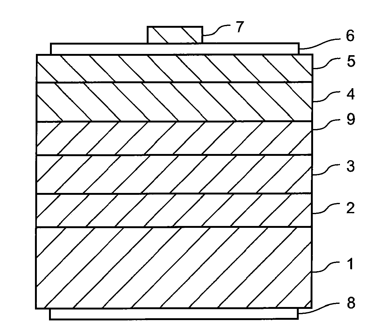
[0066]FIG. 2 is a schematic cross sectional view for explaining a method for manufacturing a ZnO based compound semiconductor device (ZnO based LED) and its structure according to the present invention.

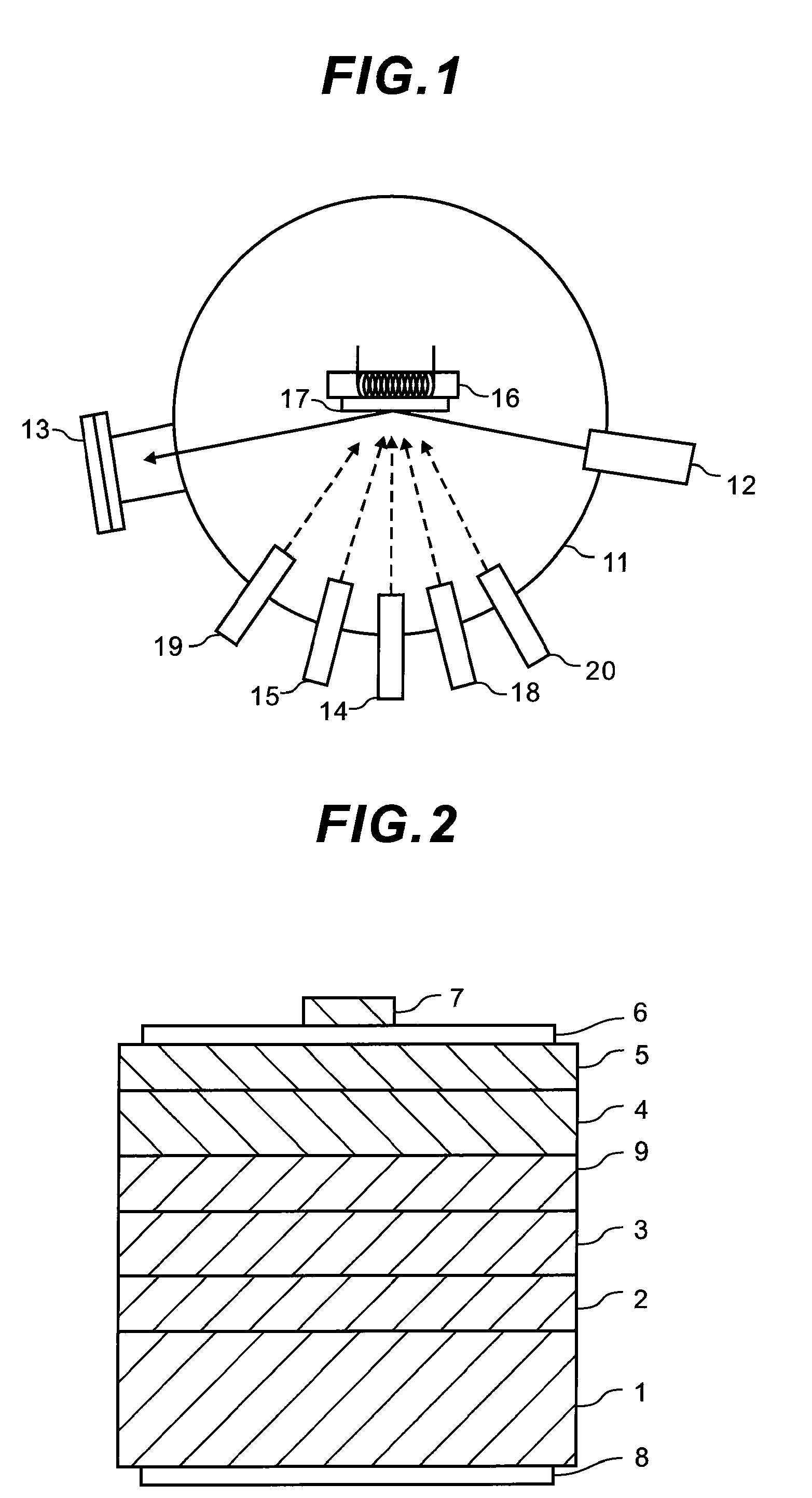
[0067]A device structure and a ZnO based compound semiconductor film according to the first embodiment of the present invention is, for example, manufactured by the molecule beam epitaxy (MBE) method explained with reference to FIG. 1. Moreover, they can be manufactured also by a well-known epitaxial growing method such as a pulsed laser deposition (PLD) method, a metal organic vapor phase epitaxy (MOVPE) method.

[0068]First, a buffer layer 2 is formed on a cleaned +c ZnO substrate 1. A thickness of the buffer layer 2 is preferably about 100 to 300 Å and is grown at 200 to 400 degrees Celsius. Thereafter, an annealing process is performed to improve a quality of the buffer layer 2 at an annealing temperature of 500 to 1000 degrees Celsius for 3 to 30 minutes.

[0069]Next, on a surface of...

second embodiment

[0120]FIG. 7 is a schematic cross sectional view for explaining a method for manufacturing a ZnO based compound semiconductor device (ZnO based LED) and its structure according to the present invention.

[0121]First, a thermal annealing process was performed to a ZnO substrate 1 and a surface of the substrate was cleaned. The thermal annealing process was performed in high vacuum of 1×10⁻⁹ Torr at 900 degrees Celsius for 30 minutes.

[0122]Then, a ZnO buffer layer 2 with a thickness of about 10 nm was formed by irradiating the Zn beam and the O radical beam onto the ZnO substrate 1 by heating the substrate temperature at 350 degrees Celsius. Continuously 20 minutes annealing process was performed by rising the substrate temperature to 800 degree Celsius to improve a crystalline quality of the buffer layer 2.

[0123]Next, a Ga—N co-doped n-type ZnO layer 31 was grown on the ZnO buffer layer 2 by simultaneously irradiating the Zn beam, the O radical beam, the Ga beam and the N radical beam ...

third embodiment

[0142]FIG. 11 is a schematic cross sectional view for explaining a method for manufacturing a sample of an n-type ZnO based compound semiconductor layer and its structure according to the present invention.

[0143]Those structures were fabricated by using the MBE method similar to the first and the second embodiments. First, a surface of the substrate 1 was cleaned and the ZnO buffer layer 2 was formed similar to the second embodiment.

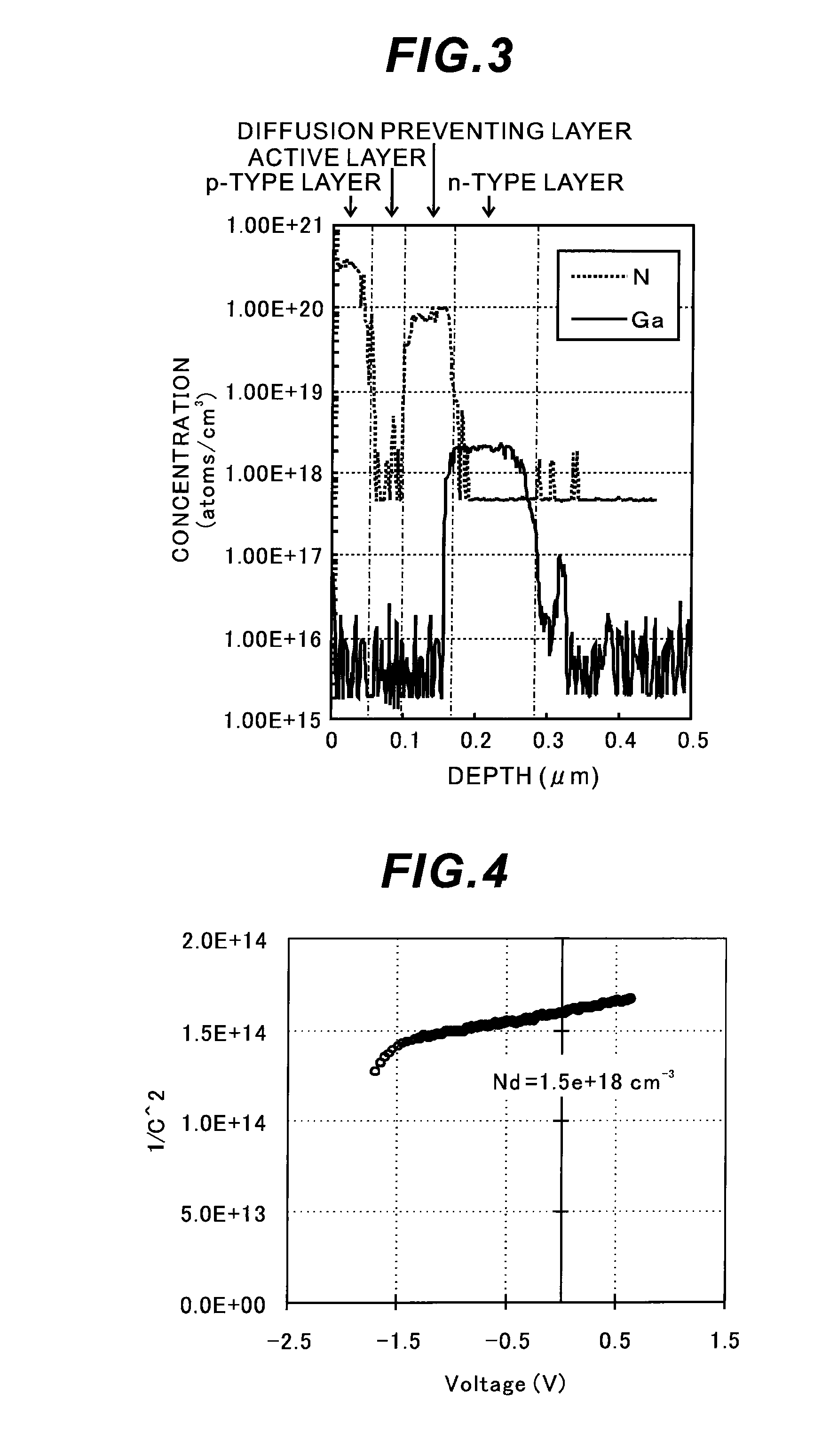
[0144]Then, the Ga—N co-doped n-type ZnO layer 31 was grown on the ZnO buffer layer 2 by simultaneously irradiating the Zn beam, the O radical beam, the Ga beam and the N radical beam onto the substrate 1 at the substrate temperature of 900 degrees Celsius. For the irradiation of the Zn beam, 7N purity Zn was used as a solid state source, and the Zn beam flux intensity (JZn) was set to 2×10¹⁵ atoms / (cm2 s). The O radical beam was irradiated by introducing 6N purity oxygen gas into the electrodeless discharge tube at 2 sccm and generating plasma at 300 W ...


PUM


Abstract

In a ZnO based compound semiconductor device, nitrogen (N) doped (Mg)ZnO:N layer is inserted as a diffusion barrier layer 9 between a ZnO based n-type layer 3 to which n-type dopants are doped and an active layer 4 or a p-type layer 5. The diffusion barrier layer 9 prevents diffusion of the n-type dopants to the active layer 4 or the p-type layer 5. Crystalline quality of the active layer 4 of the ZnO based compound semiconductor device is not deteriorated by the diffusion of the n-type dopants.

Description

[0001]This application is based on Japanese Patent Application 2009-241081, filed on Oct. 20, 2009 and Japanese Patent Application 2009-250540, filed on Oct. 30, 2009, the entire contents of which are incorporated herein by reference.BACKGROUND OF THE INVENTION[0002]A) Field of the Invention[0003]This invention relates to a zinc oxide based compound semiconductor device and more specifically relates to a zinc oxide based compound semiconductor light emitting device.[0004]B) Description of the Related Art[0005]Zinc Oxide (ZnO) is a direct band gap semiconductor with band gap energy of 3.37 eV at a room temperature and exciton binding energy of 60 meV which is relatively larger than other semiconductors. Moreover, it is characterized in that source material is cheap and harmless to a human body and environment, and so it is expected to realize an ecological light emitting device which is highly efficient and low power consuming.[0006]A p-type layer and an n-type layer are necessary fo...

Claims


Application Information

Patent Timeline
Patent Type & Authority Applications(United States)
IPC IPC(8): H01L29/12H01L21/20
CPCH01L21/0237H01L21/02403H01L21/02472H01L21/02483H01L33/285H01L21/02576H01L21/02579H01L21/02631H01L33/0087H01L21/02554
Inventor YAMAMURO, TOMOFUMIKATO, HIROYUKIOGAWA, AKIO
Owner STANLEY ELECTRIC CO LTD
Why Eureka
Try Eureka