Method of manufacturing photovoltaic cells, photovoltaic cells produced thereby and uses thereof

Inactive Publication Date: 2011-05-19
SOLAR WIND TECH +1
View PDF22 Cites 14 Cited by
  • Summary
  • Abstract
  • Description
  • Claims
  • Application Information

AI Technical Summary

Benefits of technology

[0060]According to some embodiments, the thermal treatment

Problems solved by technology

However, despite world-wide demand for environmentally friendly renewable energy sources, the high cost of manufacture of photovoltaic cells, a

Method used


Image

  • Method of manufacturing photovoltaic cells, photovoltaic cells produced thereby and uses thereof
  • Method of manufacturing photovoltaic cells, photovoltaic cells produced thereby and uses thereof
  • Method of manufacturing photovoltaic cells, photovoltaic cells produced thereby and uses thereof

Examples


Example

Example 1

Exemplary Preparation of Photovoltaic Cells

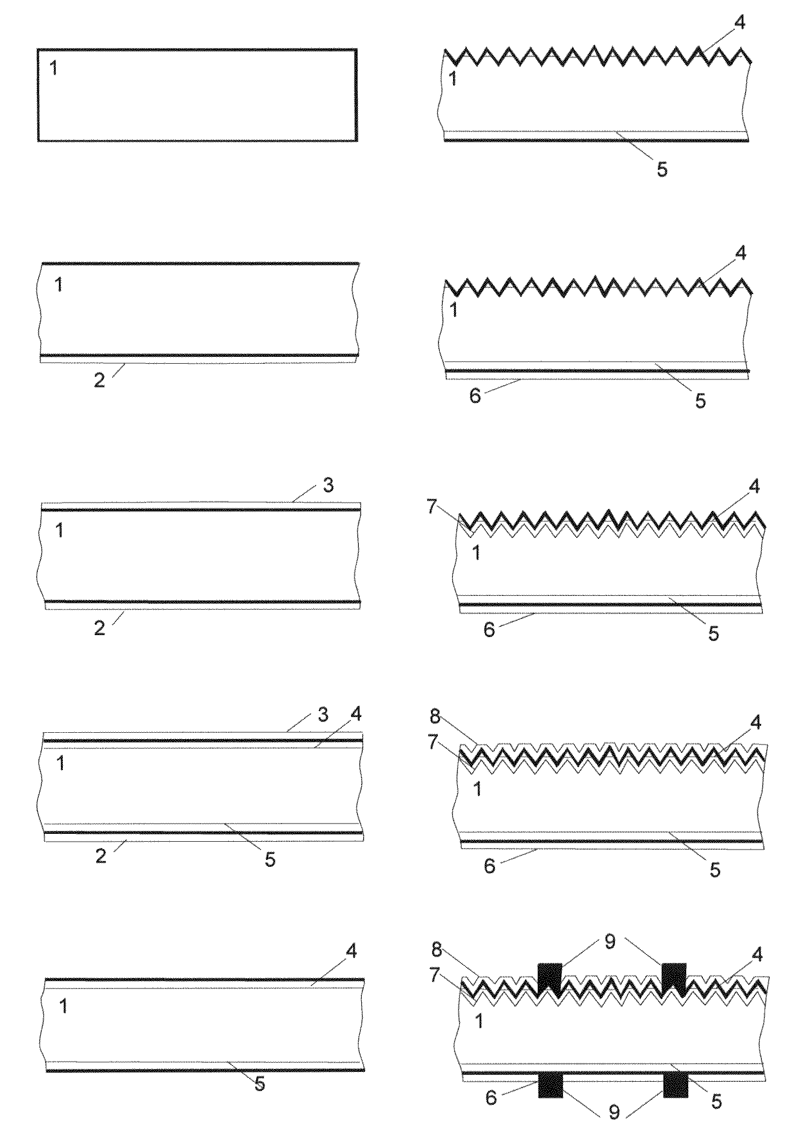
[0200]p-Type monocrystalline silicon pseudosquare substrates (125×125 mm) with a resistivity of 1.6 ohm were used. The crystal orientation of the substrate surface was [100]. Saw damage was removed by means of etching in a solution of 25% sodium hydroxide. The substrates were then washed in peroxide-ammoniac solution.

[0201]A film of silicon dioxide containing 50% (by weight) of boron oxide was applied to the back side of the substrates employing a spin-on method using a spin rate of 3,000 rpm.

[0202]The substrates were divided into 3 experimental groups of 60 substrates. Films of silicon dioxide containing 20%, 25% or 30% (by weight) P2O5 were applied to the front surface of the substrates employing the spin-on method.

[0203]Diffusion of dopants into the substrate was performed by heating for 20 minutes at a temperature of 1010° C. under a nitrogen atmosphere. The resulting p+ layer on the back side had sheet resistance of 25 ohm or ...

Example

Example 2

Effect of Antireflective Coatings on Photovoltaic Cell Performance

[0219]Photovoltaic cells were prepared as described in Example 1 with an initial n+ layer having a sheet resistance of 25 ohm and an etching depth of 8 μm. Laser p-n junction separation was performed at a distance of 0.2 mm from the edge of the substrate.

[0220]As described in Example 1, an antireflective coating was applied to the boron-doped surface before formation of the final n+ layer by phosphorus-doping, and an antireflective coating was applied to the final n+ layer following phosphorus-doping.

[0221]In one group, application of the antireflective layer on each side of the photovoltaic cell comprised forming a 75 nm layer of titanium oxide (refractive index=2.2) using an atmospheric pressure chemical vapor deposition (CVD) method, as described in Example 1.

[0222]In a second group, application of the antireflective layer on each side of the photovoltaic cell comprised forming a 60 nm layer of silicon nit...

Example

Example 3

Measurements of Effective Minority Carrier Lifetime

[0227]In order to determine the effect of silicon nitride deposition on surface recombination, the effective minority carrier lifetime was determined in p+-p-p+ structures. p+-p-p+ structures were used instead of the n+-p-p+ structure of a photovoltaic cell in order to simplify interpretation of the experimental results.

[0228]4 samples were prepared from 1 ohm·cm silicon wafers, which were doped on both sides with boron by applying a film of silicon dioxide containing 50% (by weight) of boron oxide to the back side of the substrates, and then heating for 20 minutes at a temperature of 1010° C. under a nitrogen atmosphere. A 60 nm layer of silicon nitride (refractive index=2.2) was then deposited on both sides of the wafer using a plasma-enhanced chemical vapor deposition (PECVD) method, and the wafer was then subjected to thermal treatment at a temperature of 850° C. for 20 minutes.

[0229]The lifetime values were determined ...


PUM


Abstract

Novel methods of producing photovoltaic cells are provided herein, as well as photovoltaic cells produced thereby, and uses thereof. In some embodiments, a method as described herein comprises doping a substrate so as to form a p+ layer on one side and an n+ layer on an another side, applying an antireflective coating on the p+ layer, removing at least a portion of the n+ layer, and then forming a second n+ layer, such that a concentration of the n-dopant in the second n+ layer is variable throughout a surface of the substrate.

Description

FIELD AND BACKGROUND OF THE INVENTION[0001]The present invention, in some embodiments thereof, relates to energy conversion, and, more particularly, but not exclusively, to a photovoltaic cell comprising a doped semi-conductive substrate, and to methods of producing same.[0002]Photovoltaic cells are capable of converting light directly into electricity. There is considerable hope that conversion of sunlight into electricity by photovoltaic cells will provide a significant source of renewable energy in the future, thereby enabling a reduction in the use of non-renewable sources of energy, such as fossil fuels. However, despite world-wide demand for environmentally friendly renewable energy sources, the high cost of manufacture of photovoltaic cells, as well as their limited efficiency of conversion of sunlight to electricity, has so far limited their use as a commercial source of electricity. There is therefore a strong demand for photovoltaic cells which are relatively inexpensive t...

Claims


Application Information

Patent Timeline
IPC IPC(8): H01L31/042H01L31/00H01L31/18
CPCH01L31/02168H01L31/0288Y02E10/547H01L31/1804Y02E10/52H01L31/068Y02P70/50
Inventor ZAKS, MARATKOLOMOETS, GALINASITNIKOV, ANDREYSOLODUKHA, OLEGKREININ, LEVEISENBERG, NAFTALL P.BORDIN, NINEL
Owner SOLAR WIND TECH
Why Eureka
Try Eureka