Piezoelectric device, piezoelectric device manufacturing method, and liquid discharge apparatus

a piezoelectric device and manufacturing method technology, applied in the direction of piezoelectric/electrostrictive device details, device details, device material selection, etc., can solve the problems of limited durability of piezoelectric devices, cracks or warpages, etc., to achieve excellent moisture resistance, less residual stress, and excellent durability

Active Publication Date: 2011-05-26
FUJIFILM CORP
View PDF14 Cites 12 Cited by
  • Summary
  • Abstract
  • Description
  • Claims
  • Application Information

AI Technical Summary

Benefits of technology

[0033]The present invention is based on the finding of correlation between the durability of a piezoelectric device and the average layer thickness of an interface pyrochlore oxide layer on the surface of the piezoelectric film on the side of the lower electrode, and based on the fining of a structure of a piezoelectric device which is excellent in moisture resistance, less residual stress, and excellent in durability. That is, the piezoelectric device of the present invention has a piezoelectric film of Pb containing perovskite oxide, in which the average layer thickness of an interface pyrochlore oxide layer on the surface of the piezoelectric film on the side of the lower electrode is not greater than 20 nm. According to the present invention, the durability of a piezoelectric device is improved without degrading the piezoelectric property, so that a piezoelectric device having a high piezoelectric property with favorable durability may be provided.

Problems solved by technology

In particular, Pb containing perovskite oxide films which can be formed by vapor growth methods, including sputtering method, receive attention as films having high piezoelectric properties, but still have a problem in durability.
It is known that the durability of a piezoelectric device is restricted by the deterioration in device characteristics due to residual stress in the piezoelectric film, moisture resistance of the film, and the like.
The residual stress in a piezoelectric film is likely to cause a crack or a warpage in the piezoelectric film, triggering displacement blockage of the piezoelectric device, film detachment, and the like.
Further, under a high humidity environment (in particular, a high temperature and high humidity environment), leakage current of the piezoelectric film is likely to increase due to the presence of water, leading to dielectric breakdown.
Still further, the high humidity environment causes ionization of a constituent element of the piezoelectric film which is likely to facilitate ion migration, whereby characteristics of the device are likely to be deteriorated.

Method used


Image

  • Piezoelectric device, piezoelectric device manufacturing method, and liquid discharge apparatus
  • Piezoelectric device, piezoelectric device manufacturing method, and liquid discharge apparatus
  • Piezoelectric device, piezoelectric device manufacturing method, and liquid discharge apparatus

Examples


examples

[0108]Examples and Comparative Examples according to the present invention will now be described.

example 1

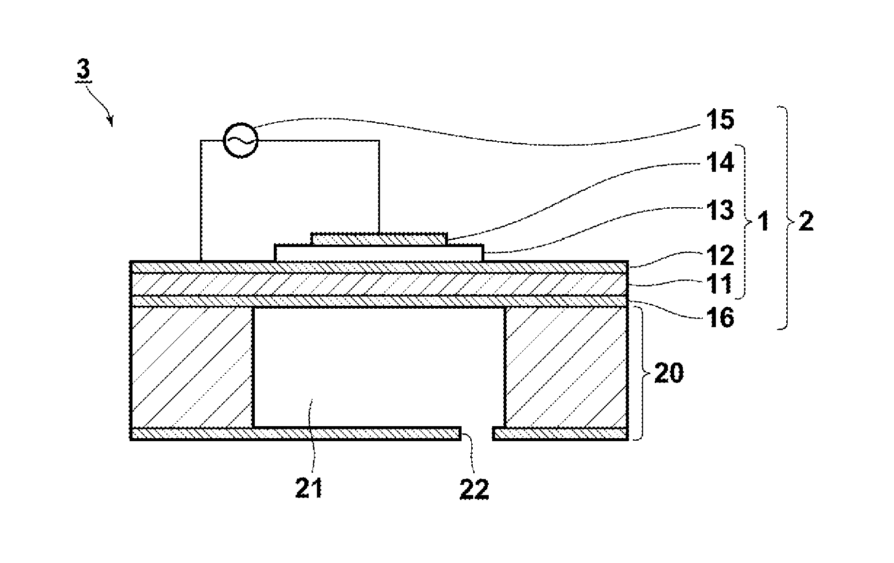
[0109]As the film forming substrate, a substrate with an electrode was provided by sequentially forming a Ti contract layer of 30 nm and a Pt lower electrode layer of 150 nm on a Si wafer. Then, a piezoelectric film (film thickness of 5 micro meters) of PZT was formed by a RF sputtering system using a target of Pb1.3Zr0.52Ti0.48O3, as Sample A, under the following conditions: film forming temperature 525 degrees Celsius, application voltage to target 2.5 W / cm2, distance between the substrate and target 60 mm, degree of vacuum 0.5 Pa, and Ar / O2 mixed atmosphere (O2 partial pressure 1.3%).

[0110]X-ray diffraction (XRD) measurements were performed on the PZT film of Sample A, and the film was confirmed to be a perovskite single-phase film, as shown in FIG. 5.

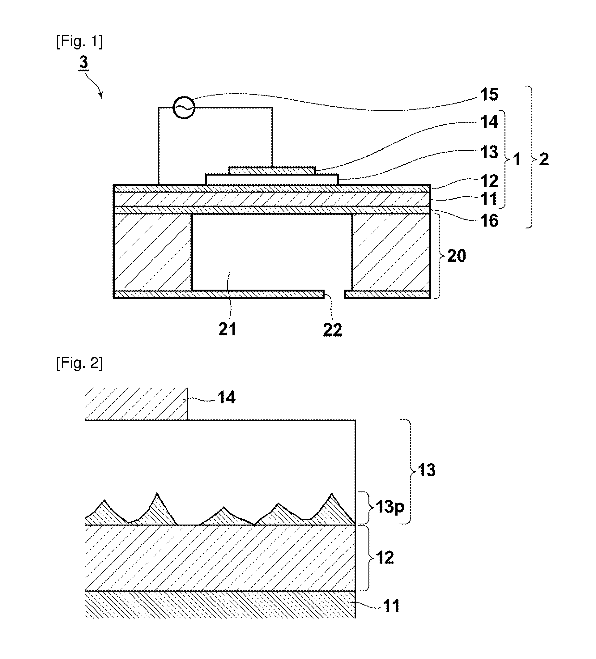
[0111]Then, a pyrochlore oxide layer at the interface of the PZT film of Sample A with the lower electrode layer was observed by HAADF-STEM. When performing the observation, Sample A was processed by a FIB (focused ion beam) system ...

example 2

[0130]A PZT film was formed on a Si substrate with an electrode in the same manner as Example 1 except that the oxygen partial pressure was set to 0.5, 2.2, 3.5, and 4.5% to examine the correlation between the average layer thickness of the interface pyrochlore oxide layer and durability life. Average layer thicknesses Th of pyrochlore oxide layers of the obtained four samples were 5 nm, 20 nm, 100 nm, and 200 nm in the ascending order of oxygen flow rate at the time of film forming.

[0131]Durability life measurements were performed in the same manner as in Example 1, the results of which are shown in FIG. 9. As shown in FIG. 9, the relationship between the average layer thickness of the interface pyrochlore oxide layer and durability life is substantially linear, and it has been confirmed that a piezoelectric device having a durability life of not less than the target durability for practical use of 10 billion cycles may be realized if the average layer thickness of the interface py...


PUM

PropertyMeasurementUnit
thicknessaaaaaaaaaa
thicknessaaaaaaaaaa
thicknessaaaaaaaaaa

Abstract

A piezoelectric device, including the following on a substrate in the order listed below: a lower electrode, a piezoelectric film which contains a Pb containing perovskite oxide represented by a general expression (P) below, and an upper electrode, in which the piezoelectric film has a layer of pyrochlore oxide on the surface facing the lower electrode, and the average layer thickness of the pyrochlore oxide layer is not greater than 20 nm.
AaBbO3  (P)
where, A: at least one type of A-site element containing Pb as a major component, B: at least one type of B-site element selected from the group consisting of Ti, Zr, V, Nb, Ta, Cr, Mo, W, Mn, Sc, Co, Cu, In, Sn, Ga, Zn, Cd, Fe, and Ni, and O: an oxygen element.

Description

TECHNICAL FIELD[0001]The present invention relates to a piezoelectric device and manufacturing method thereof, and a liquid discharge apparatus.BACKGROUND ART[0002]Piezoelectric devices that employ piezoelectric bodies having piezoelectricity in which piezoelectric bodies stretch / contract according to increase / decrease in the intensity of applied electric field are used as actuators mounted on inkjet recording heads, sensors, storage devices, and the like. Recently, in the trend toward high density and high integration of devices, reduction in film thickness of piezoelectric devices has been moved forward and development of piezoelectric devices with piezoelectric films having high piezoelectric properties has been in progress.[0003]As for piezoelectric films having high piezoelectric properties, piezoelectric films of Pb containing perovskite oxide films, such as PZT (Pb(Zr, Ti)O3: lead zirconate titanate) and the like are known. In particular, Pb containing perovskite oxide films ...

Claims


Application Information

Patent Timeline
Patent Type & Authority Applications(United States)
IPC IPC(8): B05B1/08H01L41/22H01L41/18H01L41/04B41J2/045B41J2/055B41J2/135B41J2/14B41J2/16B82Y10/00H01L41/09H01L41/187H01L41/316H01L41/39
CPCH01L41/0973C04B35/49B41J2/1646Y10T29/42H01L41/1875B41J2/161H01L41/316H10N30/1051H10N30/2047H10N30/8548H10N30/076
Inventor NIHEI, YASUKAZUFUJII, TAKAMICHIOKAMOTO, YUUICHIARAKAWA, TAKAMINAONO, TAKAYUKI
Owner FUJIFILM CORP
Why Eureka
Try Eureka