

Semiconductor light emitting device comprising high performance resins
a technology of semiconductors and resins, applied in the direction of semiconductor/solid-state device details, thermoelectric devices, solid-state devices, etc., can solve the problems of deterioration of led chips or phosphors, insufficient hardness, and easy scarring of silicon resins up to now, and achieve sufficient hardness and enhance the reaction rate
- Summary
- Abstract
- Description
- Claims
- Application Information
AI Technical Summary
Benefits of technology
Problems solved by technology
Method used
Image

Examples
embodiment 1
Embodiment 1
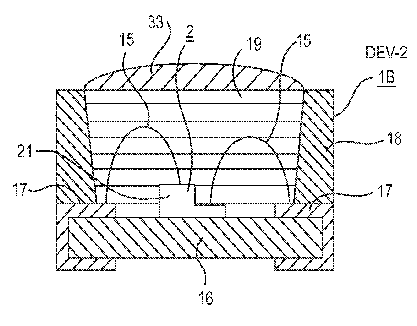
[0106]In a light emitting device DEV-1 of the present embodiment, a light emitting element 2 is surface-mounted on an insulated substrate 16 to which a printed wiring 17 is provided, as illustrated in FIG. 24. In this light emitting element 2, a p-type semiconductor layer (not shown) and n-type semiconductor layer (not shown) of the light emitting part 21 are each electrically connected to each of the printed wirings 17, 17 via each of the conductive wires 15, 15. Further, as each of the conductive wires 15, 15, one having a small cross-sectional area is used in order not to interfere with the light emitted from the light emitting element 2.
[0107]Herein, as the light emitting element 2, one emitting light at any wavelength in a range from ultraviolet region to infrared region may be used, but a gallium nitride-based LED chip is used herein. Further, in this light emitting element 2, an n-type semiconductor layer (not shown) is formed on the lower side in FIG. 24 and a p...
embodiment 2
Embodiment 2
[0115]A basic constitution of the light emitting device DEV-2 of the present embodiment is approximately the same as that of Embodiment 1, and as shown in FIG. 25, it is characterized in that a silicone member 33 which is preliminarily formed in the shape of a lens is provided on the upper side of the encapsulating part 19. Also, the components that are the same as in Embodiment 1 are denoted by the same symbols, and their explanations are omitted.
[0116]The silicone member 33 is used, for example, in the following applications.
[0117]i) A cover for blocking the light emitting device DEV-2 from external oxygen or moisture.
[0118]ii) A phosphor-containing optical member, which functions as a member for wavelength conversion of the light emitting element 2.
[0119]That is, in i), the upper sides of the light emitting element 2 and the encapsulating part 19 are blocked from external oxygen or moisture by, for example, the silicone member 33 as a transparent cover formed from gl...
example 1
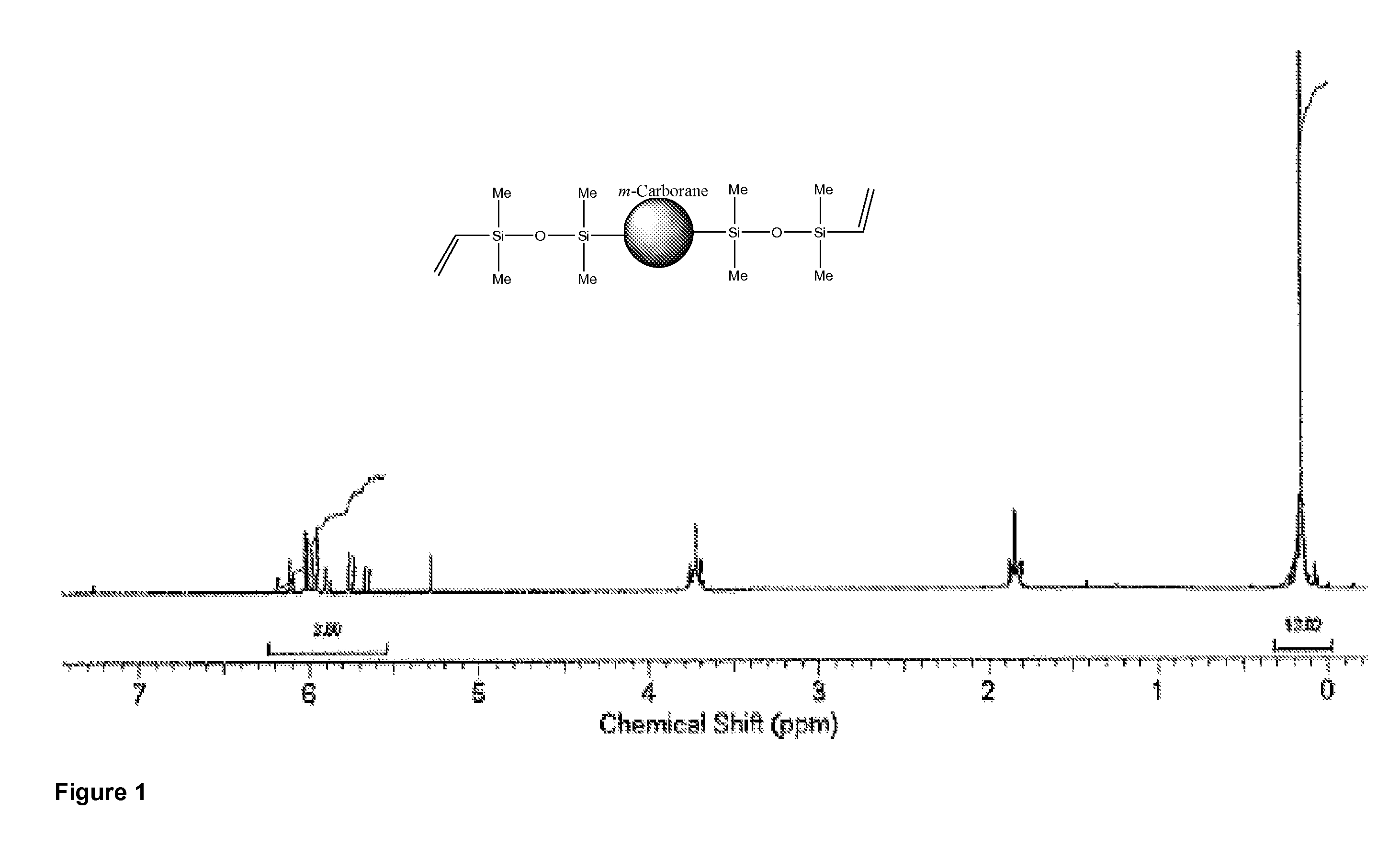
[0143]Synthesis of the Modifier Containing a Cyclic Compound Containing a 13th Group Element of the Periodic Table
(a) Synthesis of m-Carborane Containing Modifier of the Silicones for the Encapsulant of the Present Invention's Semiconductor Light Emitting Devices
[0144]The synthesis of the m-Carborane containing modifier was carried out by the reaction of 1,7-Bis(chlorotetramethyldisiloxlyl)-m-carborane (DEXSIL 300M from DEXSIL Co.) with 1M Vinyl magnesiumbromide (1.3 eq) in anhydrous THF. After the reaction was completed, excess Grignard reagent was neutralized by addition of Methanol. The mixture was then concentrated and the product was extracted into Ethyl acetate which was washed with 1M HClaq. After drying, the product was purified by column chromatography in Hexanes to obtain the m-Carborane cross-linker and the crude product was distilled at 275° C. to obtain a transparent crosslinker. (85% yield) Concentrated HClaq was used as a TLC stain. FIG. 1 shows 1H-NMR spectrum of thi...
PUM
| Property | Measurement | Unit |
|---|---|---|
| Temperature | aaaaa | aaaaa |
| Length | aaaaa | aaaaa |
| Length | aaaaa | aaaaa |
Abstract
Description
Claims
Application Information