Semiconductor device and manufacturing method of semiconductor device

a semiconductor and semiconductor technology, applied in the direction of semiconductor devices, basic electric elements, electrical appliances, etc., can solve the problems of easy non-uniformity of ni and al included in nial, difficult to form a uniform junction layer which makes a schottky junction, device destruction, etc., to achieve good ohmic junction, good surface flatness, good ohmic junction

Inactive Publication Date: 2011-06-23
SHOWA DENKO KK
View PDF9 Cites 8 Cited by
  • Summary
  • Abstract
  • Description
  • Claims
  • Application Information

AI Technical Summary

Benefits of technology

[0032]The semiconductor device according to the present invention includes the ohmic junction layer of which the root mean square roughness (rms) is 20 nm or less and which is thus excellent in surface flatness. Therefore, the uniformity of the composition in the interface between the ohmic junction layer and the first semiconductor region is good, a good ohmic junction with the first semiconductor region can be obtained, and a sufficiently high adhesiveness between the ohmic junction layer and the Schottky junction layer can be obtained. Further, the semiconductor device has good electrical characteristics in that reverse leakage current is lowered and forward surge resistance is great.
[0033]The manufacturing method of the semiconductor device according to the present invention includes a step of forming the second metal layer which is formed of the aluminum layer and the titanium layer and which includes the aluminum layer of 40 wt % or more and 60 wt % or below in terms of weight percent, on the first semiconductor region, a step of forming the ohmic junction layer which makes an ohmic junction with the first semiconductor region by alloying the second metal layer, and a step of forming the third metal layer on the second semiconductor region and alloying it at a temperature lower than the temperature for alloying the second metal layer, thereby forming the Schottky junction layer which makes a Schottky junction with the second semiconductor region by alloying the third metal layer. Therefore, it is possible to prevent aluminum from being aggregated due to the melting of aluminum included in the second metal by the alloying. For this reason, according to the manufacturing method of the semiconductor device of the present invention, the semiconductor device is realized which has an ohmic junction layer making a good ohmic junction with the first semiconductor region, excellent in surface flatness with a root mean square roughness of 20 nm or less, and giving a sufficiently high adhesiveness with the Schottky junction layer.

Problems solved by technology

In the related art, in a SiC Schottky bather diode, it is known that when a forward surge current flows, the device is destroyed even by a relatively small surge current.
However, in a case where a junction layer made of the NiAl alloy is used, it is difficult to form a uniform junction layer which makes a Schottky junction.
If the junction layer is formed in this way, there are cases where in an interface between SiC forming the n type semiconductor region and the NiAl alloy forming the junction layer, the composition of Ni and Al included in NiAl is easily non-uniform, and thus a region where a barrier height is non-uniform is generated in the junction layer which makes a Schottky junction.
For this reason, if a reverse voltage is applied to the Schottky barrier diode manufactured in this way, there are cases where an increase in leakage current is observed in a region having a low Schottky barrier and sufficient electrical characteristics cannot be obtained.
However, a metal of a single element which makes a good Schottky junction with the n type semiconductor region and makes a good ohmic junction with the p type semiconductor region has not been found until now.

Method used


Image

  • Semiconductor device and manufacturing method of semiconductor device
  • Semiconductor device and manufacturing method of semiconductor device
  • Semiconductor device and manufacturing method of semiconductor device

Examples


example

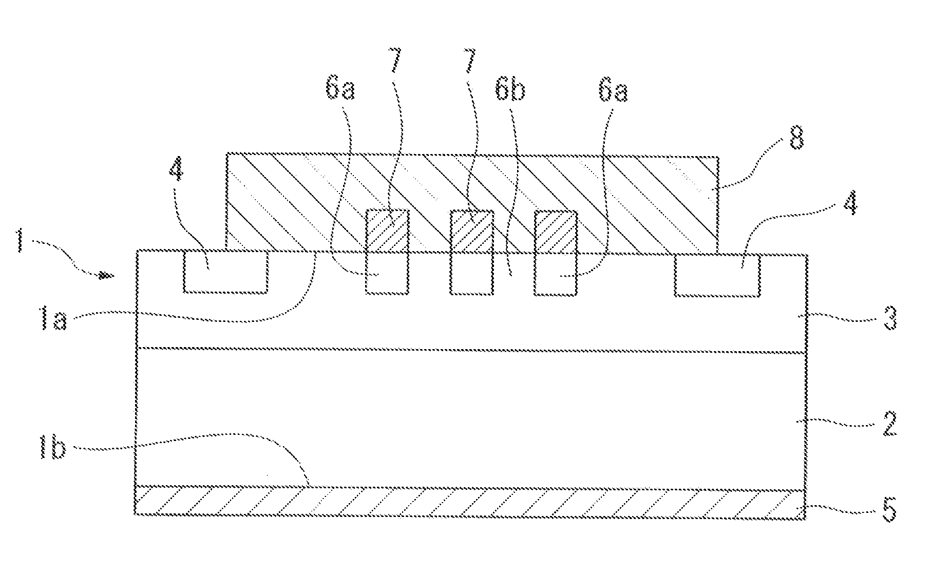
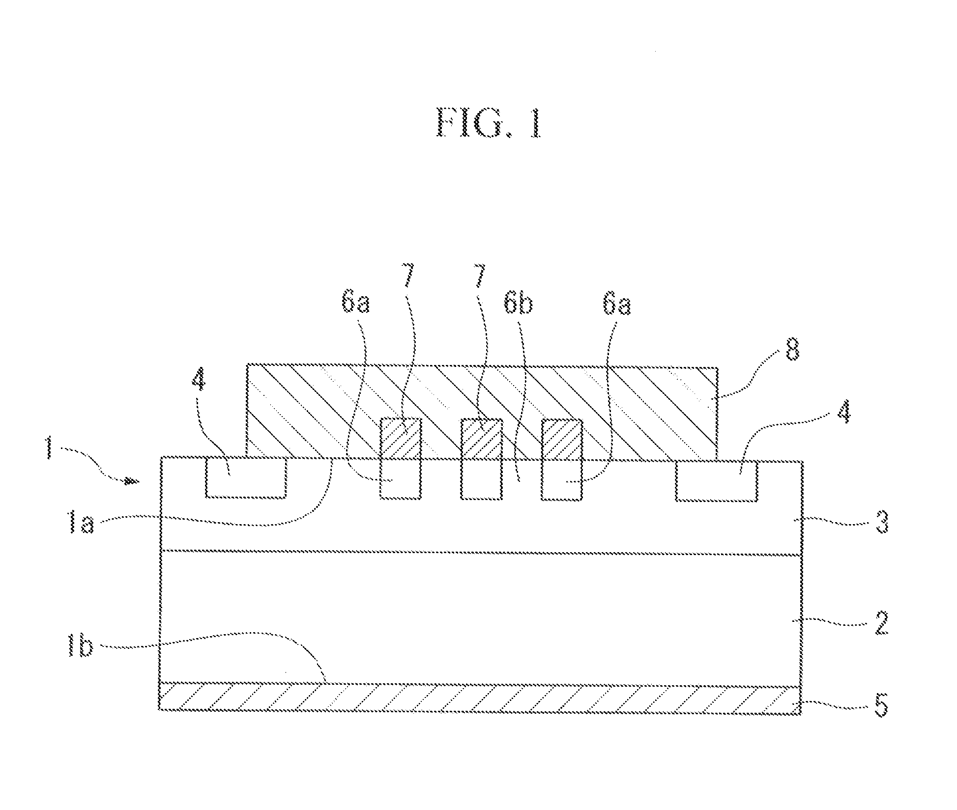
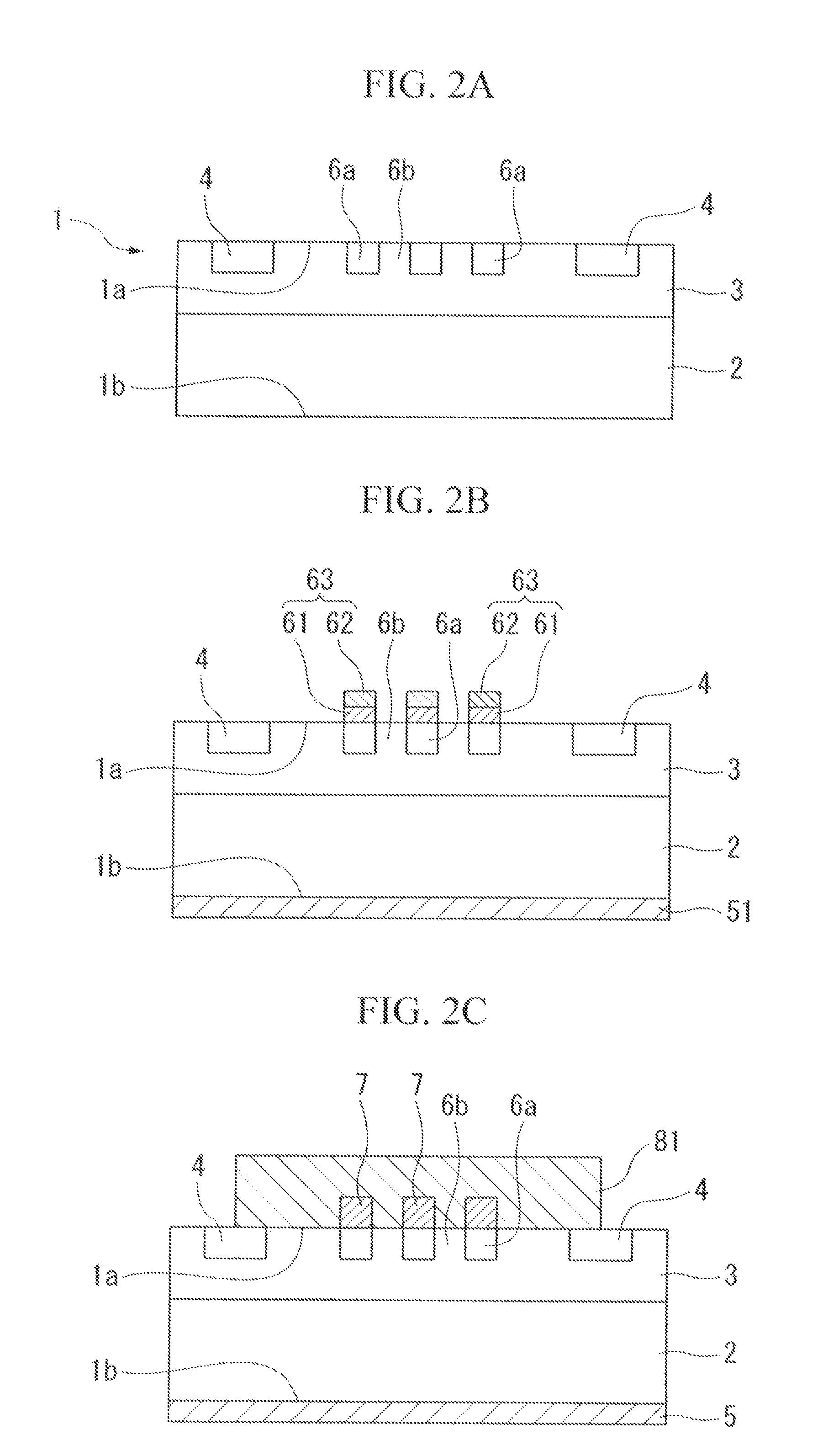
[0088]The Schottky barrier diode shown in FIG. 1 was manufactured as follows.

[0089]First, there was a preparation of the n type SiC semiconductor substrate 1 which was provided with the n+ type SiC layer 2, which is formed of an n+ type 4H—SiC monocrystalline substrate and has an impurity concentration of 2×1018 cm 3, and the n− type SiC layer 3 having an impurity concentration of 1×1016 cm-3, by forming the n− type SiC layer 3 having the thickness of 8 μm on the n+ type SiC layer 2 having a thickness of 350 μm using an n− type epitaxial layer.

[0090]Next, a SiO2 layer with the thickness of 2 μm was formed on the n− type SiC layer 3 using a plasma CVD device, and then was patterned by a photolithography process. Next, a portion of the SiO2 layer was removed to expose regions where the guard rings 4 and the first semiconductor regions 6a will be formed on the n− type SiC layer 3, and then aluminum ions were implanted into the regions with the amount of ions to be implanted of 1×1015cm...


PUM


Abstract

There is provided a semiconductor device including an ohmic junction layer which is excellent in surface flatness and uniformity of composition in an interface with a semiconductor substrate and thus can give a sufficiently high adhesiveness with a Schottky junction layer. Such a semiconductor device includes an n type SiC semiconductor substrate (1), a cathode electrode (5) that comes into ohmic contact with a main surface (1b) of one side of the SiC semiconductor substrate (1), a first semiconductor region (6a) that is made of p type SiC formed in a main surface (1a) of the other side of the SiC semiconductor substrate (1), a second semiconductor region (6b) that is made of an n type SiC formed in the main surface (1a) of the other side, an ohmic junction layer (7) that comes into ohmic contact with the first semiconductor region (1a), and a Schottky junction layer (8) that comes into Schottky contact with the second semiconductor region (6b), wherein a root mean square roughness for a surface of the ohmic junction layer (7) is 20 nm or less.

Description

TECHNICAL FIELD[0001]The present invention relates to a semiconductor device and a manufacturing method of the semiconductor device, and more particularly to a semiconductor device where an ohmic junction layer has an excellent surface flatness, and a manufacturing method of the semiconductor device.[0002]The present application contains subject matter related to that disclosed in Japanese Priority Patent Application JP 2008-212915 filed in the Japan Patent Office on Aug. 21, 2008, the entire contents of which are hereby incorporated by reference.BACKGROUND ART[0003]In the related art, in a SiC Schottky bather diode, it is known that when a forward surge current flows, the device is destroyed even by a relatively small surge current. In order to solve this problem, a device structure has been proposed in which an n type region and a p type region are arranged in parallel in one surface of an SiC semiconductor device, and injection of holes which are minority carriers is generated fr...

Claims


Application Information

Patent Timeline
Patent Type & Authority Applications(United States)
IPC IPC(8): H01L29/24H01L21/28
CPCH01L21/0485H01L21/0495H01L29/0619H01L29/872H01L29/45H01L29/47H01L29/6606H01L29/1608H01L2924/10272H01L29/861
Inventor MATSUSE, AKIHIROYANO, KOTARO
Owner SHOWA DENKO KK
Why Eureka
Try Eureka