Method for producing plasma display panel

a plasma display and manufacturing method technology, applied in the manufacture of electrode systems, gas mixture absorption, instruments, etc., can solve the problems of increasing the electric power consumption, increasing the cost of a drive circuit, increasing the discharge voltage, etc., to reduce the damage to the prebaked substrate caused by rapid cooling, the effect of reducing the prebaked substrate and reducing the vapor pressur

Inactive Publication Date: 2011-07-07
PANASONIC CORP
View PDF3 Cites 2 Cited by
  • Summary
  • Abstract
  • Description
  • Claims
  • Application Information

AI Technical Summary

Benefits of technology

[0058]In the manufacturing method for a plasma display panel according to the present invention, the highest temperature set for pre-baking in the pre-baking step (i.e. highest pre-baking temperature) is lower than the softening point of the sealing material. The temperature settings enable the organic components attributed to the paste of the sealing material to remain still as low molecular components between both the substrates even after the pre-baking step.
[0059]Furthermore, in the pre-baking step of the present invention, after one of the front substrate and the back substrate is pre-baked at the highest pre-baking temperature, a temperature of the pre-baked substrates is decreased to the room temperature in two decreasing sub-steps. In the first decreasing sub-step, compared with the subsequent second decreasing sub-step, the temperature of the pre-baked substrate is more rapidly lowered from the highest pre-baking temperature to the first temperature which is lower than the disappearance point of the binder and higher than the room temperature. This prevents the low molecular organic components included in the paste of the sealing material from being excessively dissolved upon exposure to the highest pre-baking temperature for a long period of time. As a result, the problem relating difficulty in removing the organic components excessively dissolved and incorporated in the sealing portion is avoided. Furthermore, by spending a longer time in the second decreasing sub-step than in the first decreasing sub-step, damage to the prebaked substrate caused by rapid cooling is prevented.
[0060]As mentioned above, the present invention allows the organic components attributed to the paste of the sealing material to optimally remain as the low molecular components between both the substrates. As a result, the organic components alon...

Problems solved by technology

However, the problem is that increasing the Xe partial pressure in the discharge gas as mentioned above often causes an increase in the discharge voltage, resulting in an increase in the electric power consumption.
The increase in the drive voltage also brings about a need for a pressure-proof driver, which might lead to an increase in the cost for a dr...

Method used


Image

  • Method for producing plasma display panel
  • Method for producing plasma display panel
  • Method for producing plasma display panel

Examples


embodiment

Structure of PDP Apparatus

[0080]A PDP apparatus 1000 according to the embodiment includes a PDP 1 which is connected to predetermined drive circuits 111 to 113.

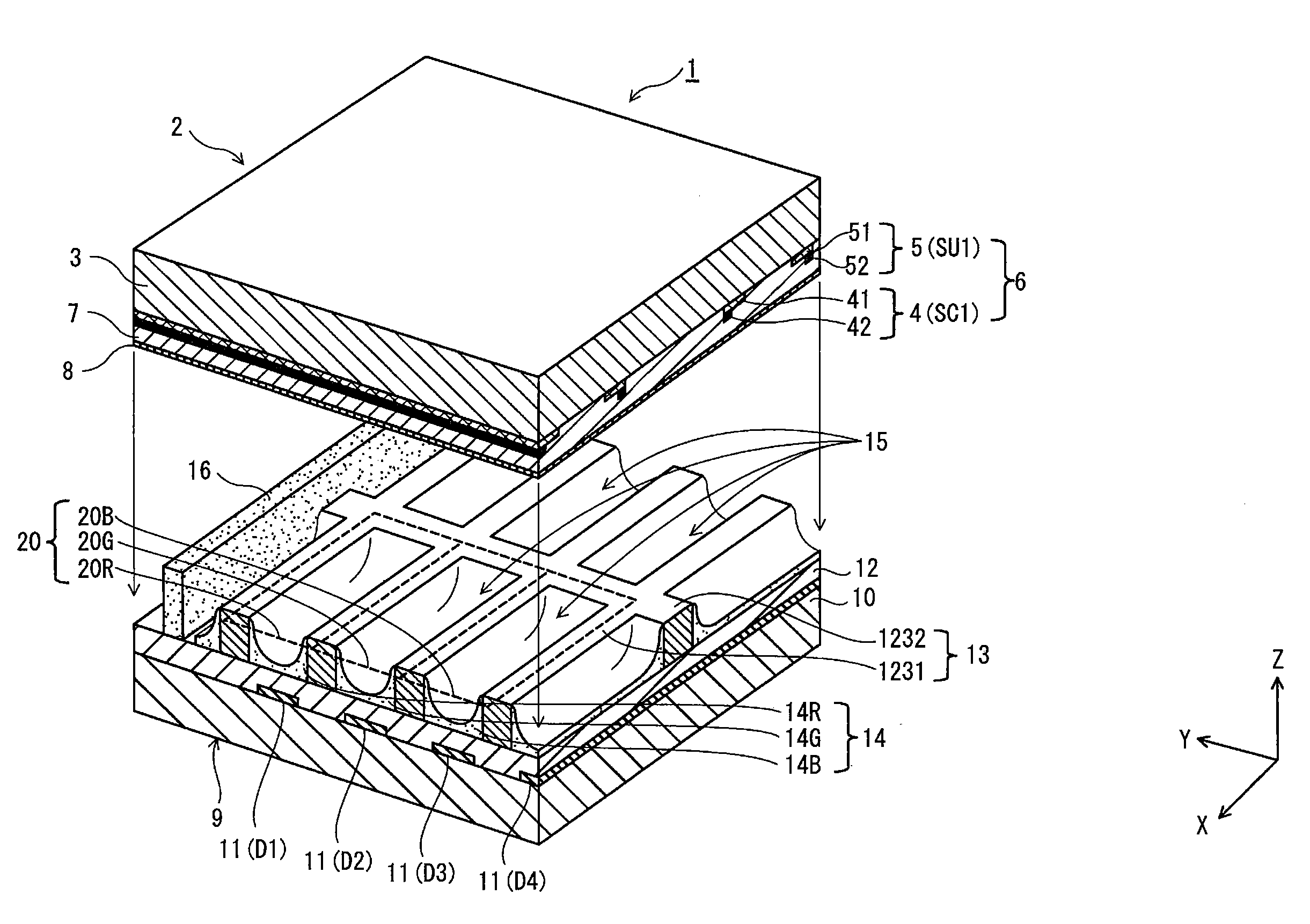
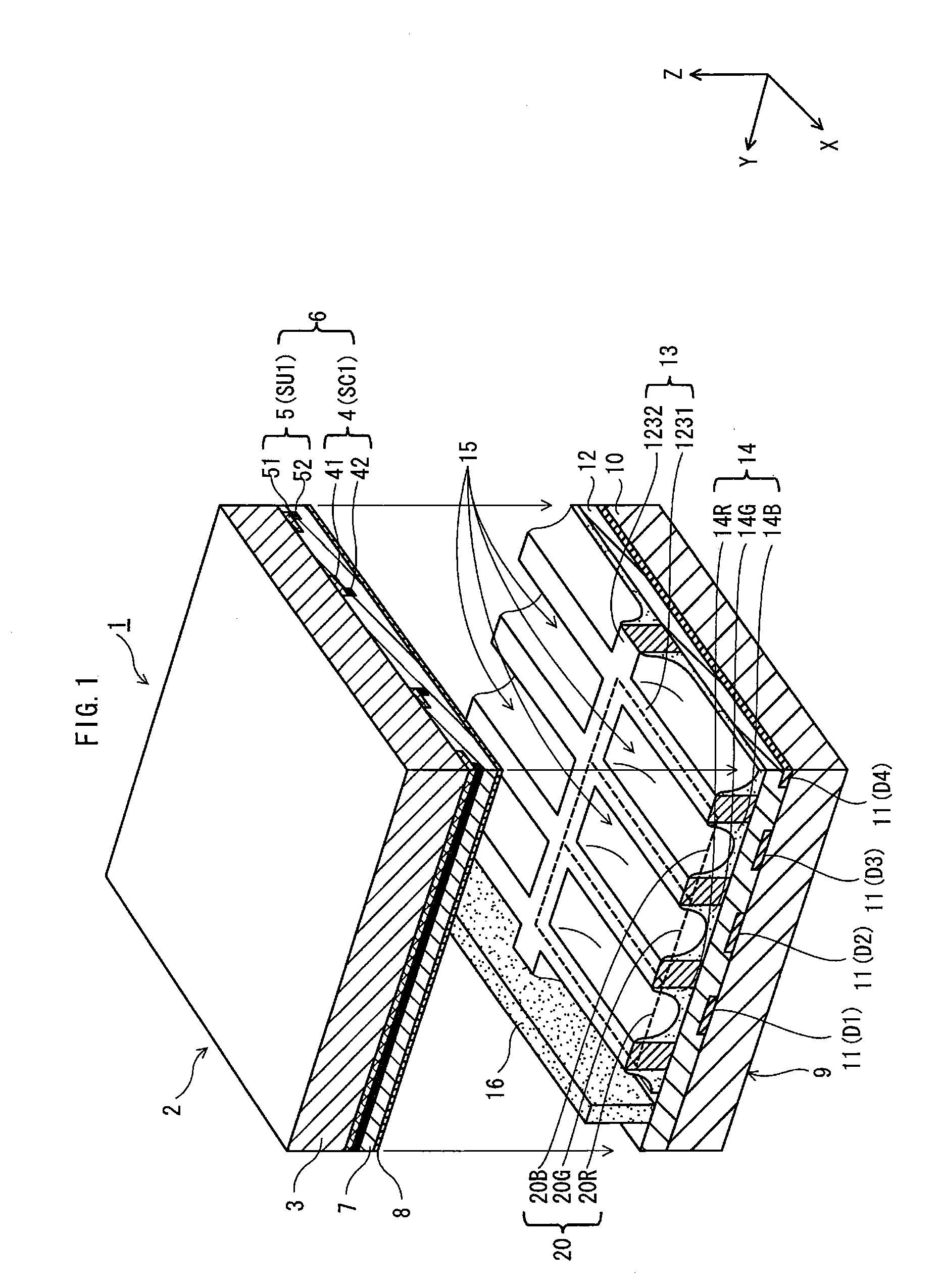
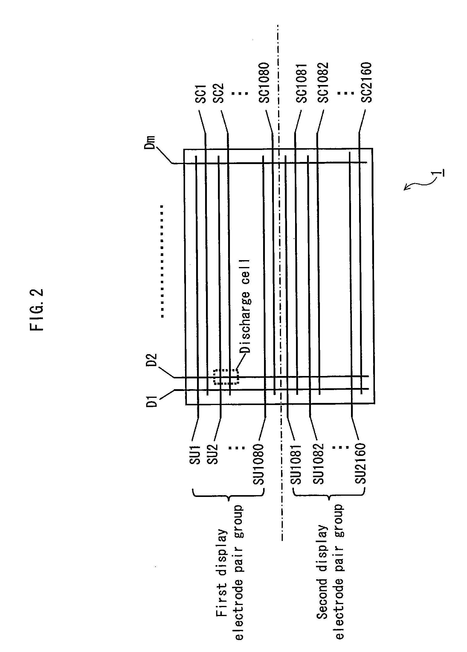
[0081]FIG. 1 is a perspective sectional view of an overall structure of the PDP 1, and partially shows an area in the vicinity of a sealing portion provided along peripheral edges of the PDP 1. FIG. 2 schematically shows an overall structure of electrode layout in the PDP 1.

[0082]As shown in FIG. 1, the PDP 1 is mainly composed of a front substrate (front panel) 2 and a back substrate (back panel) 9 that are sealed together along the peripheral edges thereof by a sealing portion 16 in a manner such that the panels 2 and 9 are superposed with a main inner surface of the front panel 2 opposing a main inner surface of the back panel 9.

[0083]The front substrate 2 includes a front substrate glass 3 as its basis. On the main surface of the front substrate glass 3, a plurality of display electrode pairs 6 (each composed of a scan el...

example 1

[0304]A PDP including small cells with a cell pitch of approximately 0.10 mm was manufactured. In the front substrate manufacturing process, the protective layer containing only MgO was obtained by distributing O2 at 0.1 (sccm) in the EB apparatus using the MgO pellet.

[0305]As the phosphors, (Y, Gd) BO3:Eu was used as red phosphors, Zn2SiO4:Mn was used as green phosphors, and BaMgAl10O17:Eu was used as blue phosphors.

[0306]As a composition of the sealing material, PbO—B2O3—RO-MO-based glass composed mainly of lead oxide-based (PbO) glass as shown in later-described Table 1 was used. The softening point of the above sealing material is 430° C., and the flow point of the sealing material is 490° C.

[0307]The highest pre-baking temperature (in the step 2 in the temperature profile of FIG. 12) in the pre-baking step was set to be 400° C. which was 30° C. lower than the softening point of the sealing material. The pre-baking step was performed for 50 minutes in the atmosphere.

[0308]In the...

example 2

[0313]The sealing step was performed in the mixed gas atmosphere consisting essentially of the N2 gas mixed with the H2 gas, with the partial pressure of the H2 gas being 3.0%, as shown in Table 1. Apart from that, settings in Example 2 are basically the same as Example 1.


PUM


Abstract

Provided is a manufacturing method that allows even a PDP having high-definition cells to exhibit excellent image display performance with reduced power consumption by effectively preventing impurities from adhering to the protective layer. Specifically, in a pre-baking step, a back substrate 9 is baked at a pre-baking temperature. Here, a highest pre-baking temperature is set to be lower than a softening point of a sealing material. The back substrate 9 is superposed on a front substrate 2. Then, a sealing step is performed in a sealing atmosphere prepared by mixing a predetermined amount of a reducing gas with a non-oxidizing gas. The above enables the impurities attributed to organic components due to a sealing material paste to remain as low molecular components, whereby the impurities are evacuated and removed in an evacuating step performed after the sealing step. This prevents adherence of the impurities to the protective layer 8.

Description

TECHNICAL FIELD[0001]The present invention relates to a manufacturing method for a plasma display panel (referred to below simply as a “PDP”), and in particular to techniques for effectively preventing impurity contamination in a protective layer and for improving a quality of the protective layer.BACKGROUND ART[0002]Plasma display panels (referred to below as “PDPs”) have attracted attention as one type of display device used for a computer and a TV. Such a PDP is a flat display apparatus that makes use of radiation caused by gas discharge. With the PDP, high-speed and high-definition display is easily possible. Moreover, size enlargement or size and weight reduction of the PDP is easily realized. Accordingly, the PDP is widely used in fields such as video display apparatuses and public information display apparatuses (see Patent Literature 1). The PDP includes direct current (DC) and alternating current (AC) types. The AC PDP, in particular a surface discharge PDP, has a high tech...

Claims


Application Information

Patent Timeline
IPC IPC(8): H01J9/20H01J9/26G09G3/28G09G3/288G09G3/291G09G3/292G09G3/293G09G3/294G09G3/296G09G3/298H01J11/12H01J11/52
CPCH01J9/241H01J9/261H01J2211/40H01J11/12H01J11/52H01J9/39
Inventor YAMAUCHI, YASUHIROSAKAI, MASAHIROFUKUI, YUSUKEOKADA, KEISUKE
Owner PANASONIC CORP
Why Eureka
Try Eureka