

NMOS transistor with enhanced stress gate
a technology of pmos transistor and gate, which is applied in the direction of transistors, electrical devices, semiconductor devices, etc., can solve the problems of adding tensile stress to nmos transistors while without degrading pmos transistors in an ic, and achieves the effect of improving tensile stress
- Summary
- Abstract
- Description
- Claims
- Application Information
AI Technical Summary
Benefits of technology
Problems solved by technology
Method used
Image

Examples
first embodiment
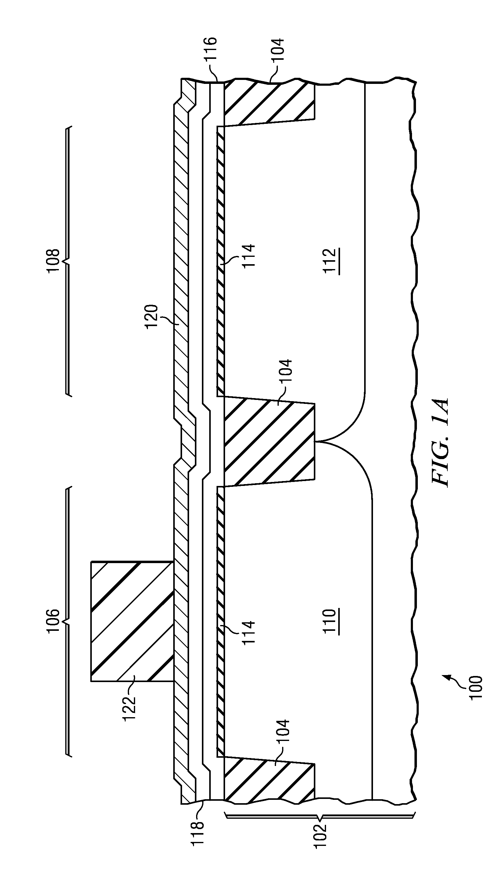
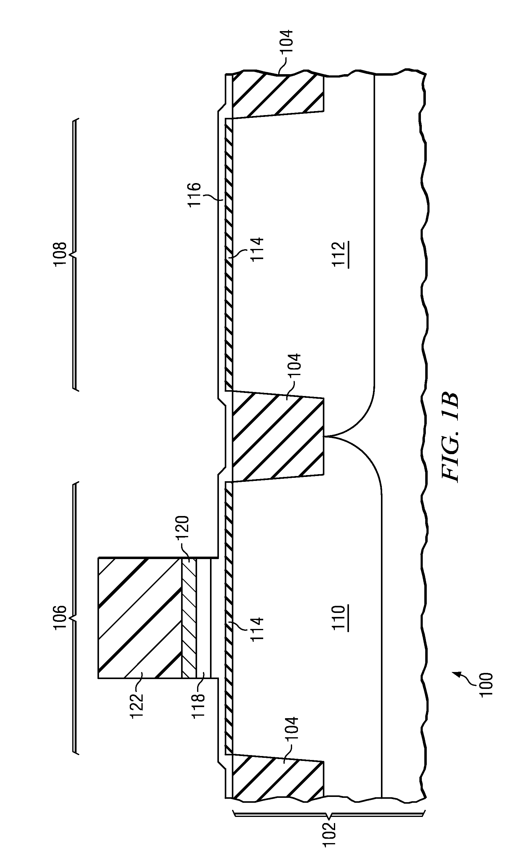
[0012]FIG. 1A through FIG. 1E are cross-sections of an IC containing an NMOS transistor including the inventive gate stack and a PMOS transistor, depicted in successive stages of fabrication. Referring to FIG. 1A, the IC 100 is formed in a substrate 102, typically p-type single crystal silicon, but possibly a silicon-on-insulator (SOI) wafer which has a layer of single crystal silicon over a buried insulating layer, or a hybrid orientation technology (HOT) wafer which has regions of different crystal orientation for different components, or any other substrate which supports fabrication of the IC 100. Elements of field oxide 104 are formed by a shallow trench isolation (STI) process sequence, in which trenches, commonly 200 to 500 nanometers deep, are etched into the IC 100, electrically passivated, commonly by growing a thermal oxide layer on sidewalls of the trenches, and filled with insulating material, typically silicon dioxide, commonly by a high density plasma (HDP) process or...
second embodiment
[0029]FIG. 2A through FIG. 2E are cross-sections of an IC containing an NMOS transistor including the inventive gate stack and a PMOS transistor, depicted in successive stages of fabrication. Referring to FIG. 2A, the IC 200 is formed in a substrate 202 with the properties described in reference to FIG. 1A. Elements of field oxide 204 are formed by an STI process sequence to isolate an area defined for an NMOS transistor 206 from an area defined for a PMOS transistor 208. A p-well 210 is formed in the substrate 202 in the NMOS area 206 by processes described in reference to FIG. 1A. An n-well 212 is formed in the substrate 202 in the PMOS area 208 by processes described in reference to FIG. 1A. A gate dielectric layer 214 as described in reference to FIG. 1A is formed on a top surface of the p-well 210 and a top surface of the n-well 212. A first layer of polysilicon 216, undoped, preferably between 2 and 10 nanometers thick, is formed on a top surface of the gate dielectric layer 2...
third embodiment
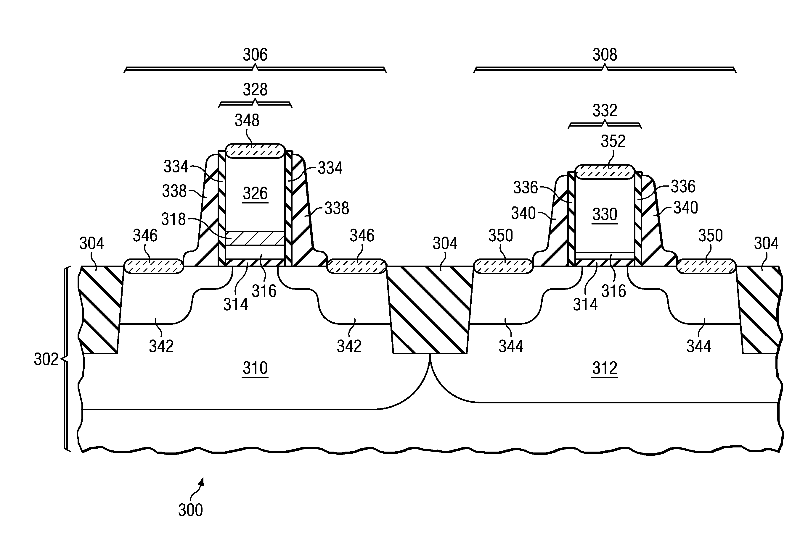
[0038]FIG. 3A through FIG. 3E are cross-sections of an IC containing an NMOS transistor including the inventive gate stack and a PMOS transistor, depicted in successive stages of fabrication. Referring to FIG. 3A, the IC 300 is formed in a substrate 302 with the properties described in reference to FIG. 1A. Elements of field oxide 304 are formed by an STI process sequence to isolate an area defined for an NMOS transistor 306 from an area defined for a PMOS transistor 308. A p-well 310 is formed in the substrate 302 in the NMOS area 306 by processes described in reference to FIG. 1A. An n-well 312 is formed in the substrate 302 in the PMOS area 308 by processes described in reference to FIG. 1A. A gate dielectric layer 314 as described in reference to FIG. 1A is formed on a top surface of the p-well 310 and a top surface of the n-well 312. A first layer of polysilicon 316, preferably between 2 and 10 nanometers thick, and which includes n-type dopants such as phosphorus, arsenic and / ...
PUM
 Abstract
Description
Claims
Application Information