

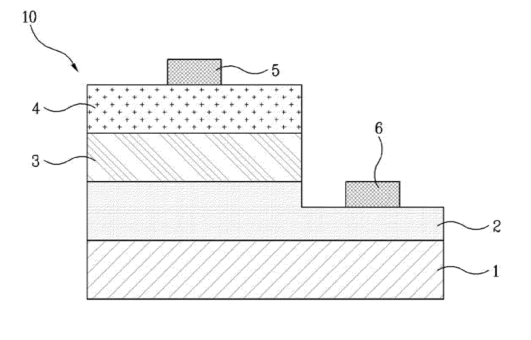
Light Emitting Diode Having Improved Light Emission Efficiency and Method for Fabricating the Same
a technology of light emission efficiency and light emission, which is applied in the direction of semiconductor/solid-state device manufacturing, electrical equipment, semiconductor devices, etc., can solve the problems of high density defects, lack of materials matched with lattice constants, and homoepitaxial growth of gan thin films, so as to improve the internal quantum efficiency of the related art, improve the overall light emission efficiency, and reduce the effect of layer defects
- Summary
- Abstract
- Description
- Claims
- Application Information
AI Technical Summary
Benefits of technology
Problems solved by technology
Method used
Image

Examples
first exemplary embodiment
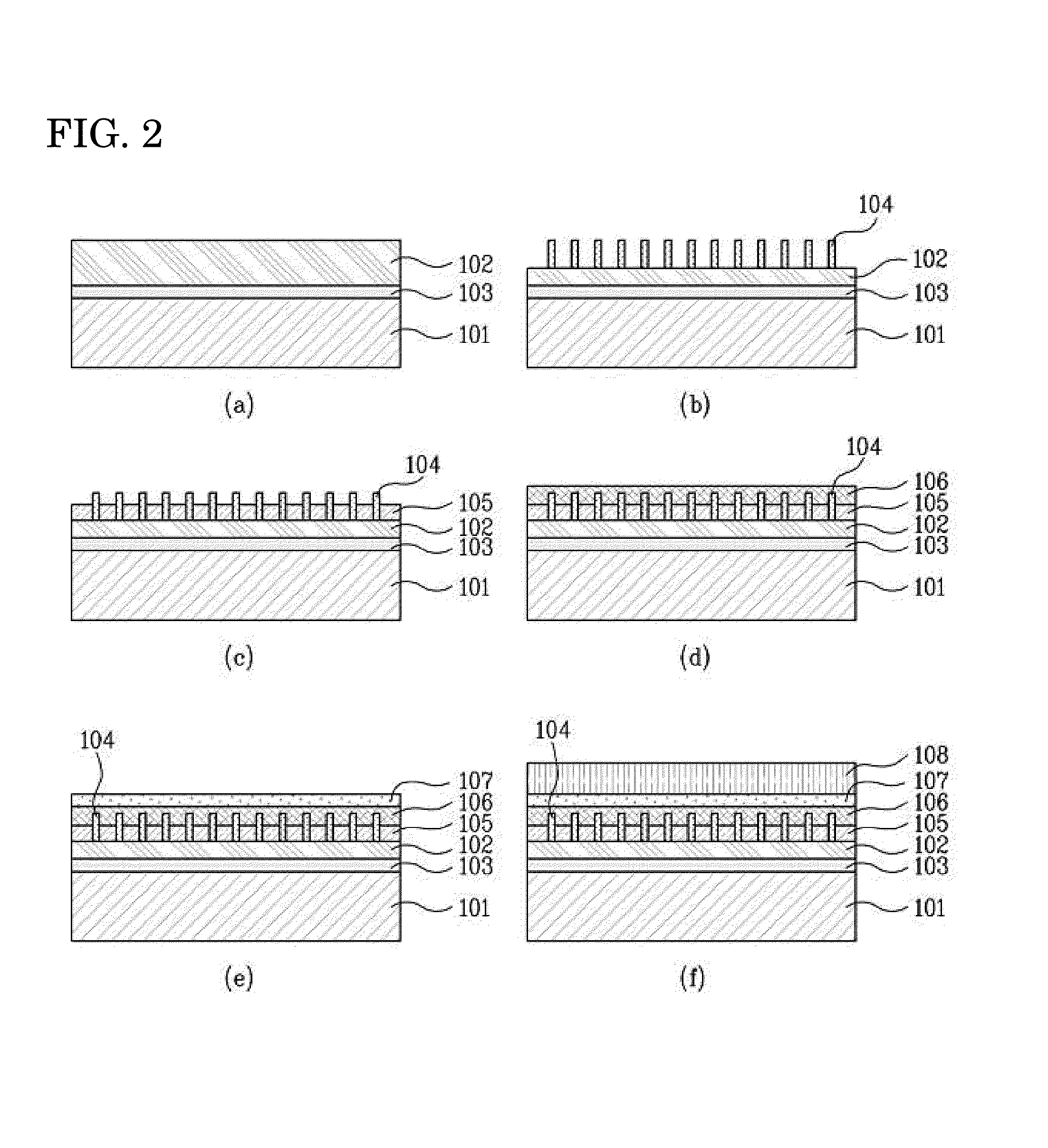
Fabrication of Wafer Sample
[0085]A sapphire substrate having a thickness of approximately 400 μm is preprocessed (heat-treated) with hydrogen gas at 1000° C. in an MOCVD (fabricated by VEECO, Model No. D-180) chamber and thereafter, a low-temperature GaN buffer layer is formed at 540° C. (thickness: approximately 30 nm). Subsequently, a wafer sample having a diameter of 2 inches is fabricated by growing an n-type GaN layer having a thickness of 2 μm at 1050° C.
[0086]PEC Etching
[0087]Etching Process (1)
[0088]The wafer sample is taken out from the chamber and thereafter, PET-etched by the PEC device (self-manufactured) shown in FIG. 3. The PEC etching process is performed in accordance with a process condition shown in Table 1 below.
TABLE 1PEC etching parametersConditionsElectrolyteKOH (0.02M)Applied voltage 2 VEtching time 30 minutesIntensity of ultraviolet rays350 mW
[0089]FIG. 6 is a photograph of a scanning electron microscope (SEM) showing porosity including nano rods on the surfa...
second exemplary embodiment
[0105]Electroluminescence (EL) Evaluation
[0106]Electrical characteristics are measured at the time of evaluating EL of each of the LED fabricated in accordance with the first exemplary embodiment and a control group (an LED fabricated in the same method as the first exemplary embodiment except PEC etching and the metal layer forming process are performed) and the measurement results are displayed by an I-V curve shown in FIG. 12. As shown in the figure, in the case of the EL measurement, the LED according to the first exemplary embodiment has a forward voltage of 4.4V, while the control group has a forward voltage of 4.6. Therefore, they are substantially similar to each other. As a result, the existence of the metal layer has no particular influence on the electrical characteristics.
[0107]Meanwhile, the EL characteristics of the LED fabricated according to the first exemplary embodiment and the control group is evaluated and the evaluation results are shown by an L-I curve shown in...
third exemplary embodiment
[0110]In order to verify whether or not the defects are reduced in the LED according to the exemplary embodiment of the present invention, the density of the defect (threading dislocations) of each of the LED fabricated in accordance with the first exemplary embodiment and a control group (an LED fabricated by the same method as the first exemplary embodiment except PEC etching and the metal layer forming process are performed) is measured.
[0111]Each of the LED samples is wet-etched in molten KOH at 350° C. for 5 minutes. In this case, the defect portions are etched during wet etching and the number of defects per unit area is counted and calculated.
[0112]The surfaces of the first exemplary embodiment and the control group in accordance with the experiment are shown in FIGS. 15A and 15B, respectively. On the basis of the measurement result, the defect density of the first exemplary embodiment is approximately 5.2×10⁵ / cm2, while the defect density of the control group is approximatel...
PUM
 Abstract
Description
Claims
Application Information