Method of manufacturing silicon carbide semiconductor device

a semiconductor device and silicon carbide technology, applied in the direction of individual semiconductor device testing, semiconductor/solid-state device testing/measurement, instruments, etc., can solve the problems of preventing or reducing the step bunching, adhesion and leakage characteristics may deteriorate, and surface roughness called step bunching on the surface of silicon carbide wafers, etc., to prevent or reduce the step bunching, the effect of preventing the evaporation of silicon and high accuracy

Active Publication Date: 2011-09-15
MITSUBISHI ELECTRIC CORP
View PDF9 Cites 13 Cited by
  • Summary
  • Abstract
  • Description
  • Claims
  • Application Information

AI Technical Summary

Benefits of technology

[0014]An object of the present invention is to provide a method of manufacturing a silicon carbide semiconductor device capable of measuring th

Problems solved by technology

However, when a silicon carbide wafer is annealed at a high temperature, a surface roughness called step bunching occurs in a surface of the silicon carbide wafer.
The step bunching thus formed becomes an obstacle to the formation of a gate oxide film on the silicon carbide wafer after the annealing process, and also becomes an obstacle to the formation of a gate electrode on the gate oxide film.
For example, there is a possibility that adhesion and leakage characteristics may deteriorate because a boundary sur

Method used


Image

  • Method of manufacturing silicon carbide semiconductor device
  • Method of manufacturing silicon carbide semiconductor device
  • Method of manufacturing silicon carbide semiconductor device

Examples


embodiment 1

Preferred Embodiment 1

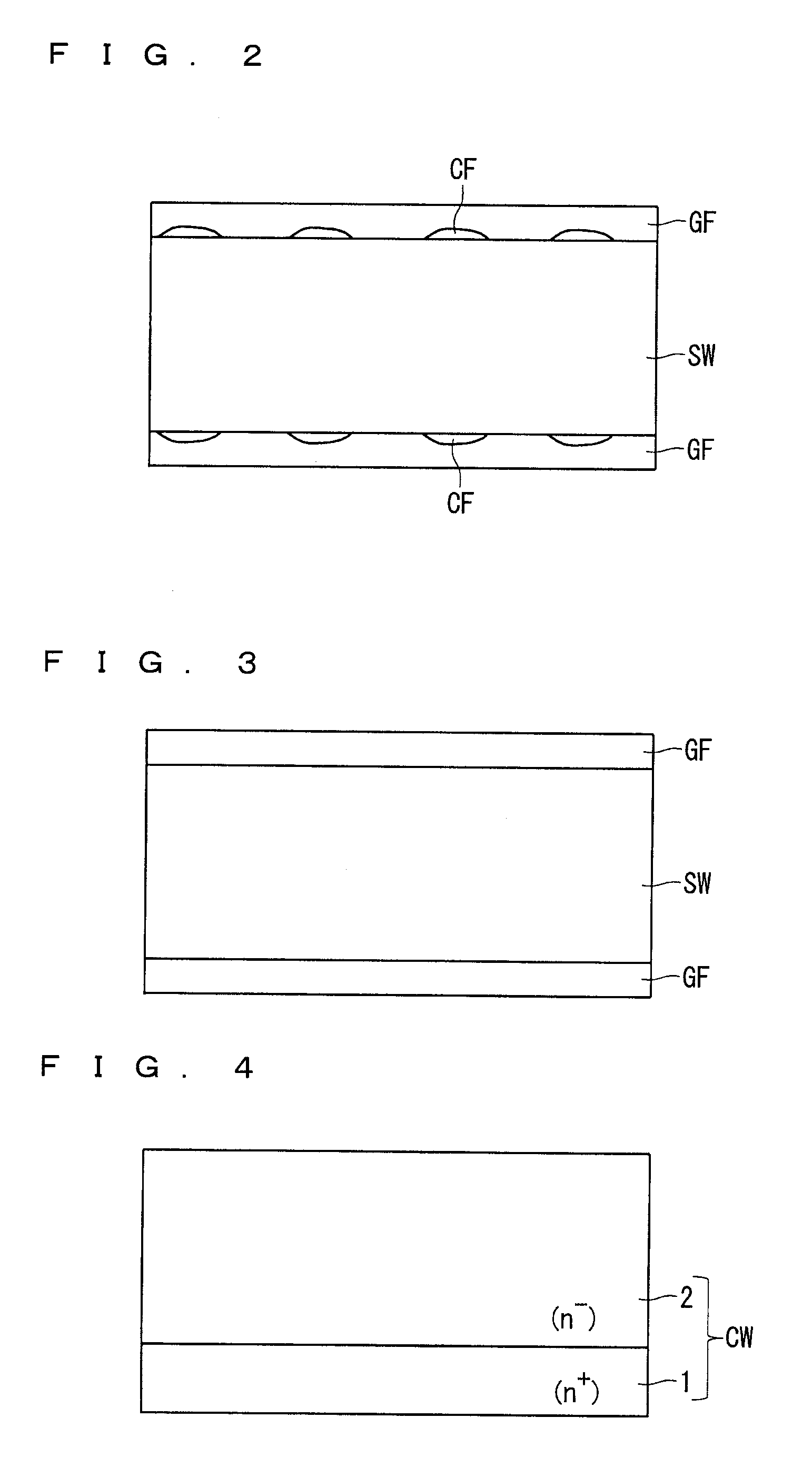
[0026]In the present status, a silicon carbide wafer is very expensive, and therefore from the viewpoint of avoiding the use of silicon carbide wafer as a film thickness monitor for a protective film, the present inventors have reached the technical idea of using a silicon wafer instead of a silicon carbide wafer, as a film thickness monitor.

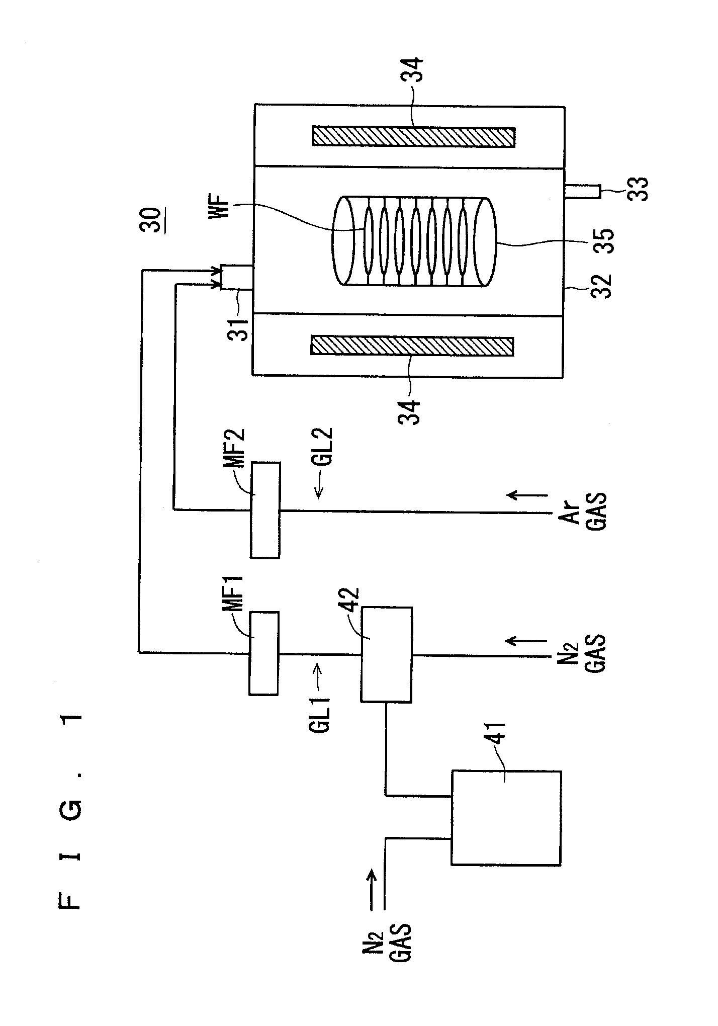
[0027]FIG. 1 shows an outline of a film forming device for forming a graphite film which serves as a protective film on a silicon carbide wafer. Here, it is assumed that the graphite film is formed (deposited) by a chemical vapor deposition (CVD), and a configuration of a CVD device 30 which is a typical film forming device is shown.

[0028]As shown in FIG. 1, the CVD device 30 includes a gas introduction part 31, a film forming furnace 32, a gas discharge part 33, a heater 34, and a substrate holder 35. The gas introduction part 31 is for the introduction of a source gas or the like which is used to form a graphite film. The...

embodiment 2

Preferred Embodiment 2

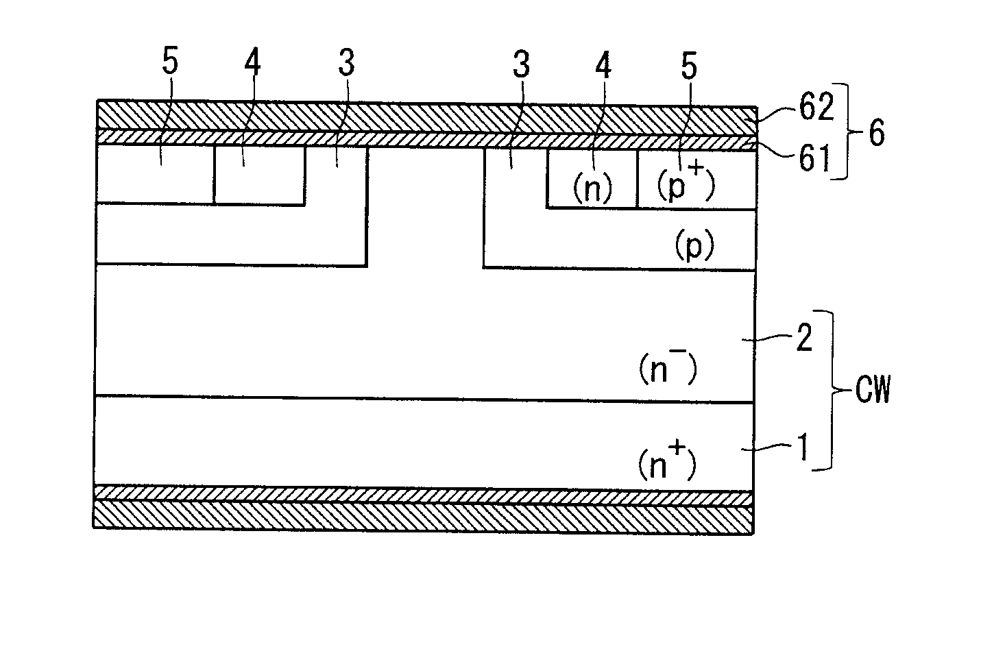
[0043]A method of manufacturing a silicon carbide semiconductor device according to a preferred embodiment 2 of the present invention will be described with reference to FIGS. 4 to 8.

[0044]FIGS. 4 to 6 are diagrams sequentially showing manufacturing steps of a power MOSFET (Power Metal Oxide Semiconductor Field Effect Transistor), up to a step of forming a graphite film.

[0045]Here, the term “MOS” was formerly used to express a layered structure of metal-oxide-semiconductor, and is supposed to be named after the initial letters of Metal-Oxide-Semiconductor. However, particularly in a field effect transistor (hereinafter simply referred to as a “MOS transistor”) having a MOS structure, materials of a gate insulating film and a gate electrode have been improved from the viewpoint of the recent integrations and improvement in the manufacturing process.

[0046]For example, in a MOS transistor, mainly from the viewpoint of the source and drain being formed in a self-al...


PUM

PropertyMeasurementUnit
Temperatureaaaaaaaaaa

Abstract

A wafer WF is mounted in a substrate holder, and the substrate holder is placed in a film forming furnace. The film forming furnace is evacuated by a vacuum pump through a gas discharge part to remove remaining oxygen as completely as possible. Then, a temperature in the film forming furnace is heated to a range of 800° C. to 950° C. under reduced pressure while an inert gas such as Ar or helium (He) is being introduced through a gas introduction part. When the temperature reaches this temperature range, an inflow of the inert gas is stopped. Vaporized ethanol is introduced as a source gas into the film forming furnace through the gas introduction part, thus forming a graphite film on an entire surface of the wafer WF.

Description

BACKGROUND OF THE INVENTION[0001]1. Field of the Invention[0002]The present invention relates to a method of manufacturing a silicon carbide semiconductor device.[0003]2. Description of the Background Art[0004]Silicon carbide (SiC) enables manufacturing of a silicon carbide semiconductor device having higher breakdown voltage characteristics as compared with silicon (Si) which has been conventionally used, and is expected to provide a high-power semiconductor device for the next generation. In manufacturing a silicon carbide semiconductor device using such silicon carbide, to control a conductive type and conductivity, an n-type or p-type impurity ion is implanted in a silicon carbide wafer having a silicon carbide layer formed on a silicon carbide substrate by epitaxial growth, and after the ion implantation, in order to activate the implanted ion and additionally recover a crystal defect formed by the ion implantation, an annealing process step is performed in which the ion-implan...

Claims


Application Information

Patent Timeline
IPC IPC(8): H01L21/66
CPCC23C16/325C23C16/56H01L21/046H01L22/12Y10S438/931H01L29/1608H01L29/66068H01L29/7802H01L29/0657H01L21/20H01L21/265H01L22/00
Inventor UDA, YUKIOSEKIYA, KOICHIKOBAYASHI, KAZUOTARUI, YOICHIRO
Owner MITSUBISHI ELECTRIC CORP
Why Eureka
Try Eureka