

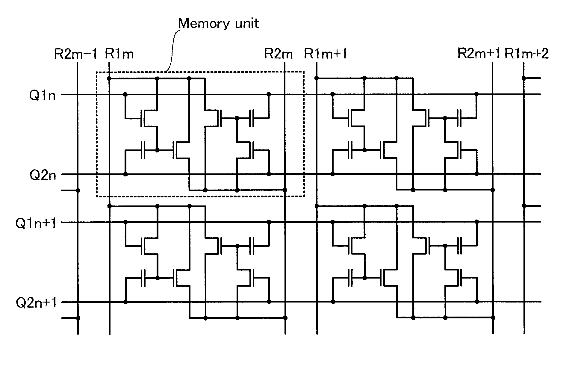
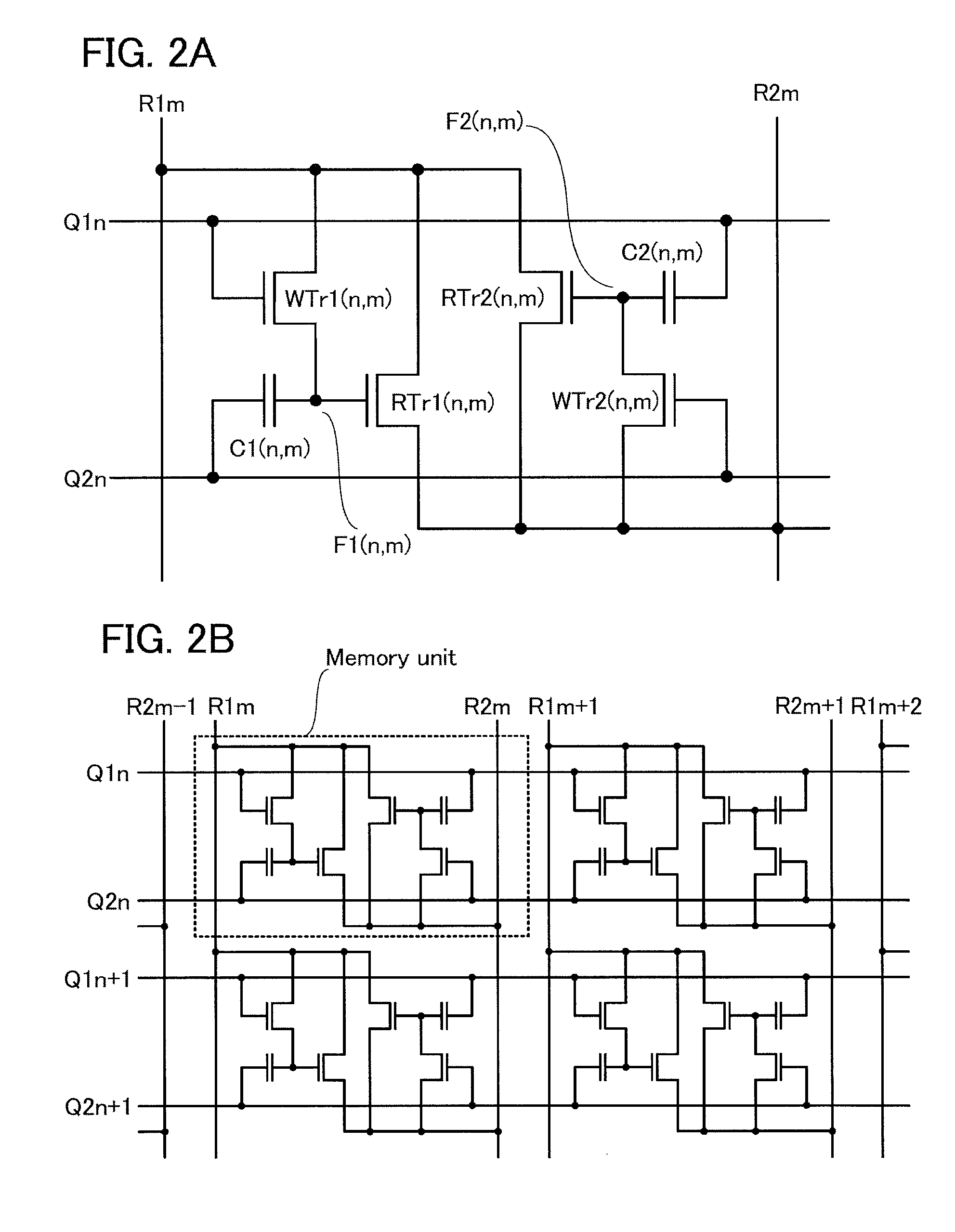
Semiconductor memory device
- Summary
- Abstract
- Description
- Claims
- Application Information
AI Technical Summary
Benefits of technology
Problems solved by technology
Method used
Image

Examples
embodiment 1
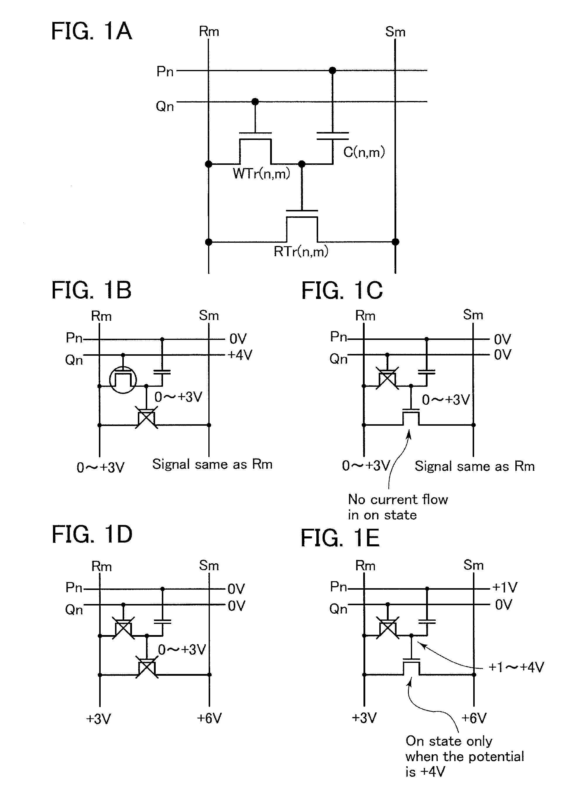
[0102]In this embodiment, an example of operation of the semiconductor memory device illustrated in FIG. 1A will be described with reference to FIGS. 1B to 1E. Note that specific values of potentials are given below for the purpose of aid for understanding a technical idea of the present invention. Needless to say, such values are changed in accordance with various characteristics of a transistor, a capacitor, or the like, or for convenience of the practitioner. Further, the semiconductor memory device illustrated in FIG. 1A can write or read data using a method other than a method described below.
[0103]Here, the writing transistor WTr(n,m) and the reading transistor RTr(n,m) are both n-channel transistors. The writing transistor WTr(n,m) and the reading transistor RTr(n,m) are turned on (current flows through the transistors) when the potential of the gate becomes higher than the potential of either the source or the drain by 1 V or more, and the writing transistor WTr(n,m) and the...
embodiment 2
[0127]In this embodiment, an example of operation of the semiconductor memory device illustrated in FIG. 11A will be described with reference to FIGS. 11B to 11E. Note that specific values of potentials are given below for the purpose of aid for understanding a technical idea of the present invention. Needless to say, such values are changed in accordance with various characteristics of a transistor, a capacitor, or the like, or for convenience of the practitioner. Further, the semiconductor memory device illustrated in FIG. 11A can write or read data using a method other than a method described below.
[0128]Here, the writing transistor WTr(n,m) is an n-channel transistor, and the reading transistor RTr(n,m) is a p-channel transistor. The writing transistor WTr(n,m) is turned on (current flows through the transistor) when the potential of the gate becomes higher than the potential of either the source or the drain by 1 V or more, and the writing transistor WTr(n,m) is in an off state...
embodiment 3
[0150]In this embodiment, an example of the shape and a manufacturing method of the semiconductor memory device described in Embodiment 1 will be described. In this embodiment, an oxide semiconductor containing gallium and indium is used for the writing transistor and a single crystal silicon semiconductor is used for the reading transistor. Therefore, the writing transistor is stacked over the reading transistor.
[0151]That is, an insulated gate transistor including a single crystal silicon semiconductor which is provided over a single crystal silicon substrate is used as the reading transistor and a transistor in which an oxide semiconductor is used is formed thereover as the writing transistor. Note that although an example in which a semiconductor memory device is formed over a single crystal silicon substrate is described in this embodiment, the semiconductor memory device can be provided over another kind of substrate.
[0152]An example of layout of a memory cell of the semicondu...
PUM
 Abstract
Description
Claims
Application Information