Method for manufacturing composite piezoelectric substrate and piezoelectric device

a piezoelectric substrate and composite piezoelectric technology, applied in the direction of piezoelectric/electrostrictive device details, device details, generators/motors, etc., can solve the problem of difficult commercial manufacture of large composite piezoelectric substrates, adversely affecting the piezoelectricity of composite piezoelectric substrates, and the material of a supporting substrate cannot have much less linear expansion coefficients

Active Publication Date: 2011-11-17
MURATA MFG CO LTD
View PDF7 Cites 73 Cited by
  • Summary
  • Abstract
  • Description
  • Claims
  • Application Information

AI Technical Summary

Benefits of technology

To overcome the problems described above, preferred embodiments of the present invention provide a method for manufacturing a piezoelectric...

Problems solved by technology

However, implanted ions remaining in the piezoelectric thin film adversely affect the piezoelectricity of the composite piezoelectric substrate.
During these heating processes, a high thermal stress at the interface between the supporting substrate and the piezoelectric thin film can cause problems, such as the detachment or cracking of the piezoelectric thin film.
Such defects in the piezoelectric thin film are particularly noticeable during the manufacture of large composite piezoelectric substrates, making it difficult to commercially manufacture large composite piezoelectric substrates.
However, due to the constraint on the coefficient of linear expansion, the material of a supporting substrate cannot have a coeffi...

Method used


Image

  • Method for manufacturing composite piezoelectric substrate and piezoelectric device
  • Method for manufacturing composite piezoelectric substrate and piezoelectric device
  • Method for manufacturing composite piezoelectric substrate and piezoelectric device

Examples


first preferred embodiment

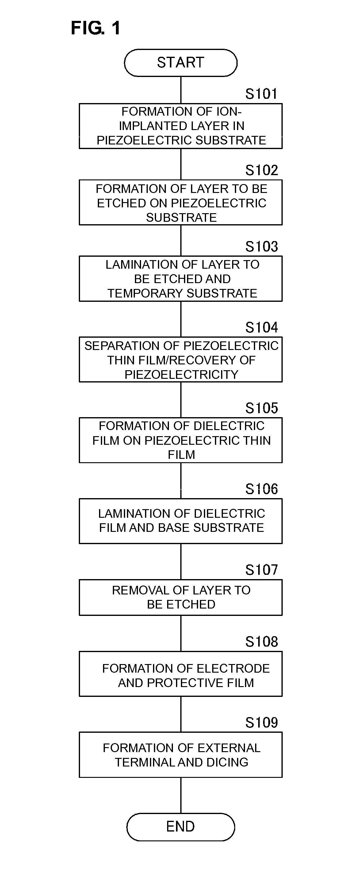
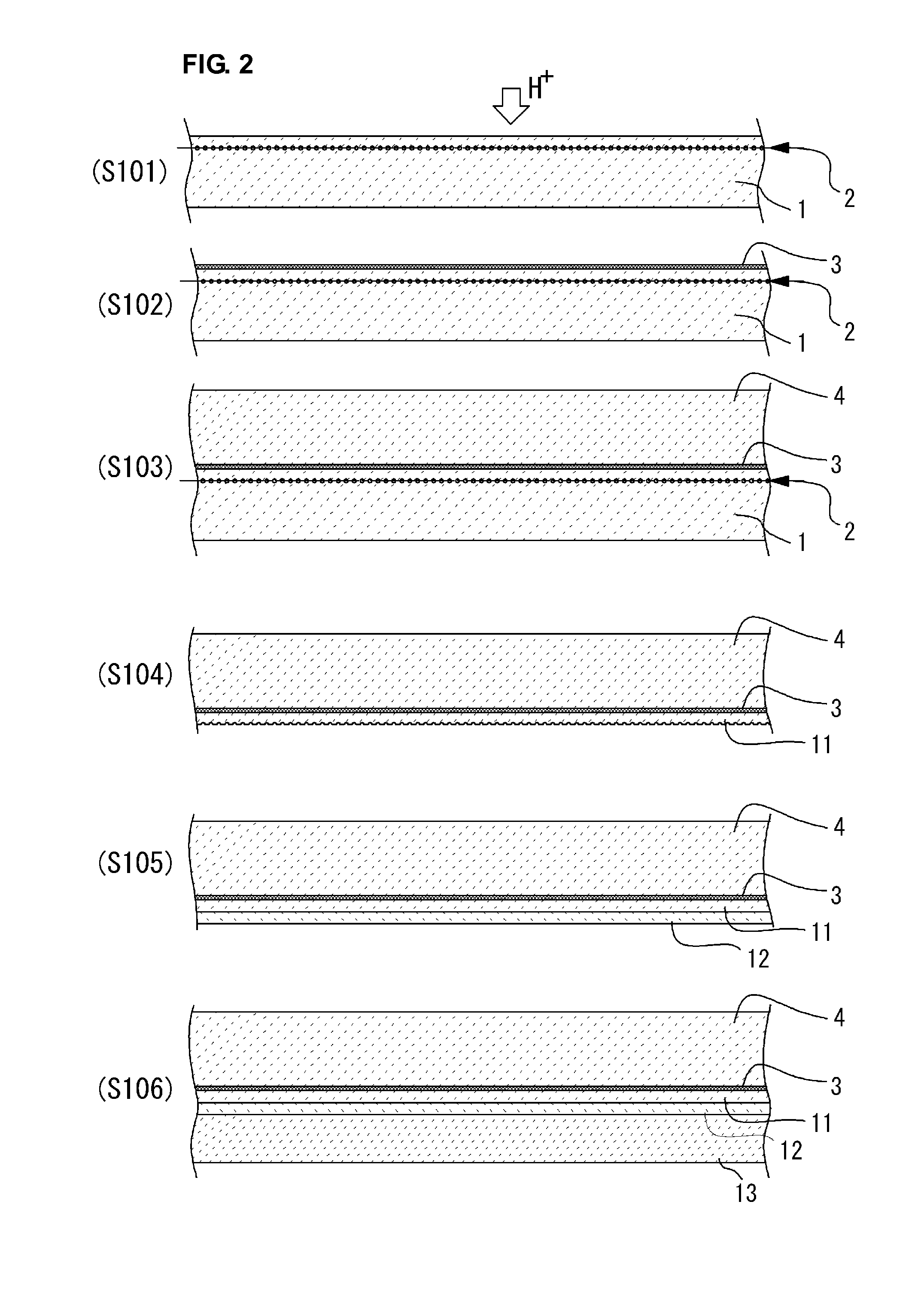
A method for manufacturing a surface acoustic wave device including a composite piezoelectric substrate according to a first preferred embodiment of the present invention will be described below with reference to FIGS. 1 to 4B. FIG. 1 is a flow chart of a method for manufacturing a surface acoustic wave device according to the first preferred embodiment. FIGS. 2 and 3 are schematic cross-sectional views of manufacturing steps described in the flow chart in FIG. 1.

First, an ion implantation step is performed on a piezoelectric substrate 1 (FIGS. 1 and 2: S101). The piezoelectric substrate 1 is preferably a single-crystal substrate made of a piezoelectric substance, for example. In the ion implantation step, ions are implanted into a flat main surface of the piezoelectric substrate 1 to form an ion-implanted portion 2 in the main surface.

The piezoelectric substrate 1 is preferably a LiTaO3 (LT) single-crystal substrate, for example. The piezoelectric substrate 1 can be divided by the ...

second preferred embodiment

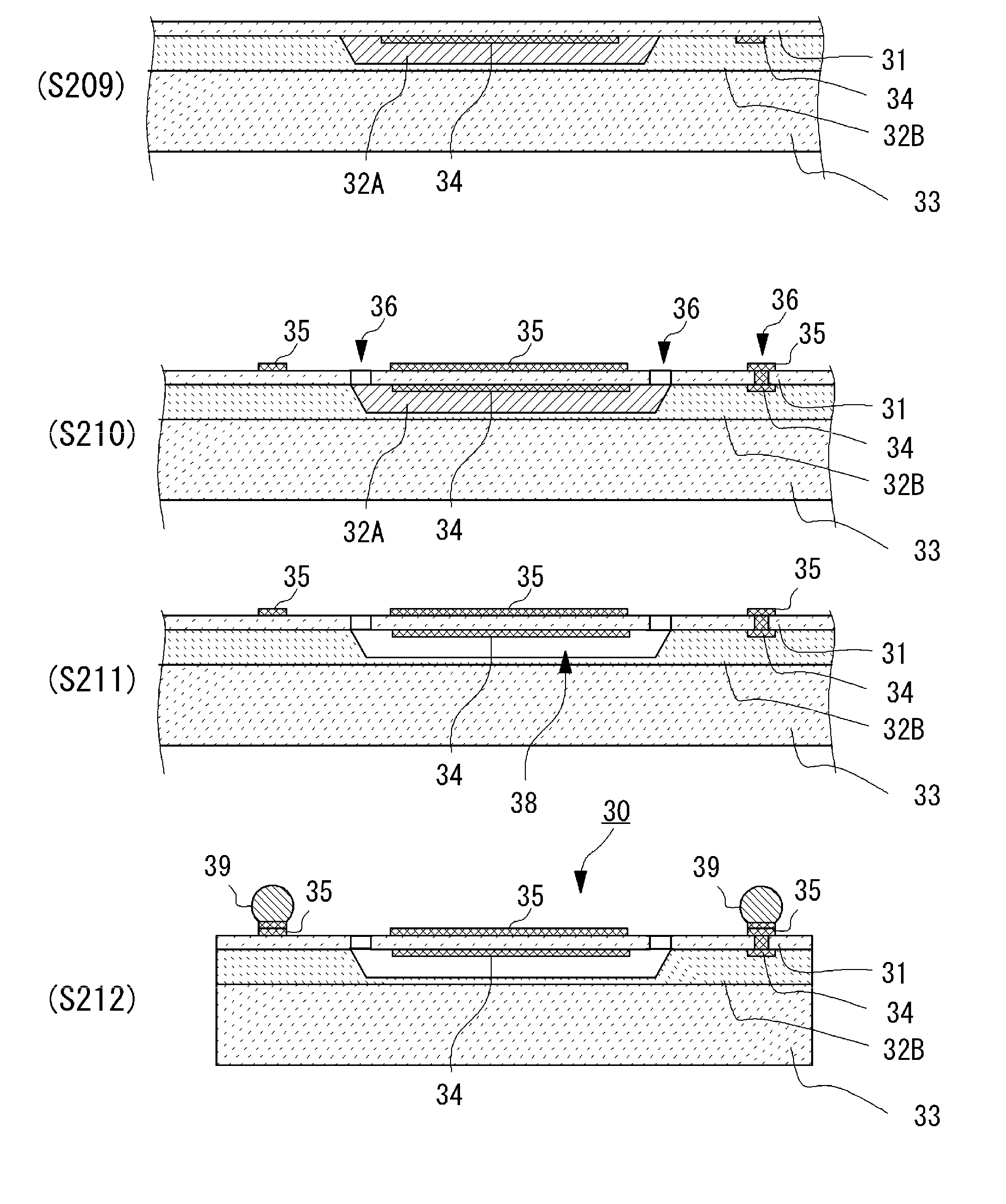
A method for manufacturing a bulk wave device including a composite piezoelectric substrate according to a second preferred embodiment of the present invention will be described below with reference to FIGS. 5 to 8B. FIG. 5 is a flow chart of a method for manufacturing a bulk wave device according to the second preferred embodiment. FIGS. 6 and 7 are schematic cross-sectional views of manufacturing steps described in the flow chart in FIG. 5.

In the same or substantially the same manner as in the first preferred embodiment, an ion implantation step is performed first (FIG. 5: S201). An etching layer forming step is then performed (FIG. 5: S202). A temporary supporting step is then performed (FIG. 5: S203). A heating step is then performed (FIGS. 5 and 6: S204). A temporary supporting substrate including a layer to be etched 23 and a temporary substrate 24 is formed on the ion-implanted surface of a piezoelectric thin film 31 preferably having a thickness of approximately 1 μm, for ex...

third preferred embodiment

A method for manufacturing a gyro device including a composite piezoelectric substrate according to a third preferred embodiment of the present invention will be described below with reference to FIGS. 9 to 11. A gyro device vibrates a silicon diaphragm with a piezoelectric vibrator, and detects the Coriolis force acting on the silicon diaphragm during rotation with the piezoelectric vibrator. A method for manufacturing a tuning-fork gyro device will be described below. The tuning-fork gyro device includes a piezoelectric vibrator and a silicon diaphragm. The piezoelectric vibrator includes a piezoelectric thin film and a drive electrode. The piezoelectric vibrator is disposed on the silicon diaphragm.

FIG. 9 is a flow chart of a portion of a method for manufacturing a gyro device according to the third preferred embodiment. FIGS. 10 and 11 are schematic cross-sectional views of manufacturing steps described in the flow chart in FIG. 9.

In substantially the same manner as in the first...


PUM

PropertyMeasurementUnit
Temperatureaaaaaaaaaa
Dielectric polarization enthalpyaaaaaaaaaa
Concentrationaaaaaaaaaa

Abstract

A piezoelectric device is manufactured in which the material of a supporting substrate can be selected from various alternative materials. Ions are implanted into a piezoelectric substrate to form an ion-implanted portion. A temporary supporting substrate is formed on the ion-implanted surface of the piezoelectric substrate. The temporary supporting substrate includes a layer to be etched and a temporary substrate. The piezoelectric substrate is then heated to be divided at the ion-implanted portion to form a piezoelectric thin film. A supporting substrate is then formed on the piezoelectric thin film. The supporting substrate includes a dielectric film and a base substrate. The temporary supporting substrate is made of a material that produces a thermal stress at the interface between the temporary supporting substrate and the piezoelectric thin film less than the thermal stress at the interface between the supporting substrate and the piezoelectric thin film.

Description

BACKGROUND OF THE INVENTION1. Field of the InventionThe present invention relates to a method for manufacturing a composite piezoelectric substrate including a piezoelectric thin film and a piezoelectric device including the composite piezoelectric substrate. More particularly, the present invention relates to a method for manufacturing a composite piezoelectric substrate in which a piezoelectric thin film is subjected to heat treatment and a piezoelectric device including the composite piezoelectric substrate.2. Description of the Related ArtVarious piezoelectric devices that utilize piezoelectric thin films are being developed.Piezoelectric devices include a composite piezoelectric substrate including a piezoelectric thin film and a supporting substrate (see, for example, Japanese Unexamined Patent Application Publication No. 2002-534886).In accordance with Japanese Unexamined Patent Application Publication No. 2002-534886, the supporting substrate may be made of sapphire, silicon...

Claims


Application Information

Patent Timeline
IPC IPC(8): H01L41/047H01L41/22H01L41/04H03H3/02H03H3/08H03H9/145H03H9/17
CPCH03H3/02H03H3/08H03H9/02015H03H9/173H03H9/174Y10T29/42H03H2003/023H01L41/312H01L41/332H01L41/29H01L41/37H03H2003/021H10N30/072H10N30/082H03H9/25H10N30/01H01L21/76259H01L21/76254H10N30/092H10N30/06
Inventor IWAMOTO, TAKASHI
Owner MURATA MFG CO LTD
Why Eureka
Try Eureka